Double gated fin transistors and methods of fabricating and operating the same

a technology of double gated fins and transistors, applied in the field of non-planar transistors, can solve the problems of increasing difficulty in operation and control of transistors, gate or other structure construction, and construction of gates or other structures

Active Publication Date: 2012-05-24
MICRON TECH INC
View PDF2 Cites 20 Cited by
  • Summary
  • Abstract
  • Description
  • Claims
  • Application Information

AI Technical Summary

Problems solved by technology

High aspect ratio fins typically are desirable but challenging to construct.
As the dimensions of the fin structures and the space between each fin are reduced, construction of gates or other structures, and operation and control of the transistors may be increasingly difficult.

Method used


Image

  • Double gated fin transistors and methods of fabricating and operating the same
  • Double gated fin transistors and methods of fabricating and operating the same
  • Double gated fin transistors and methods of fabricating and operating the same

Examples


Embodiment Construction

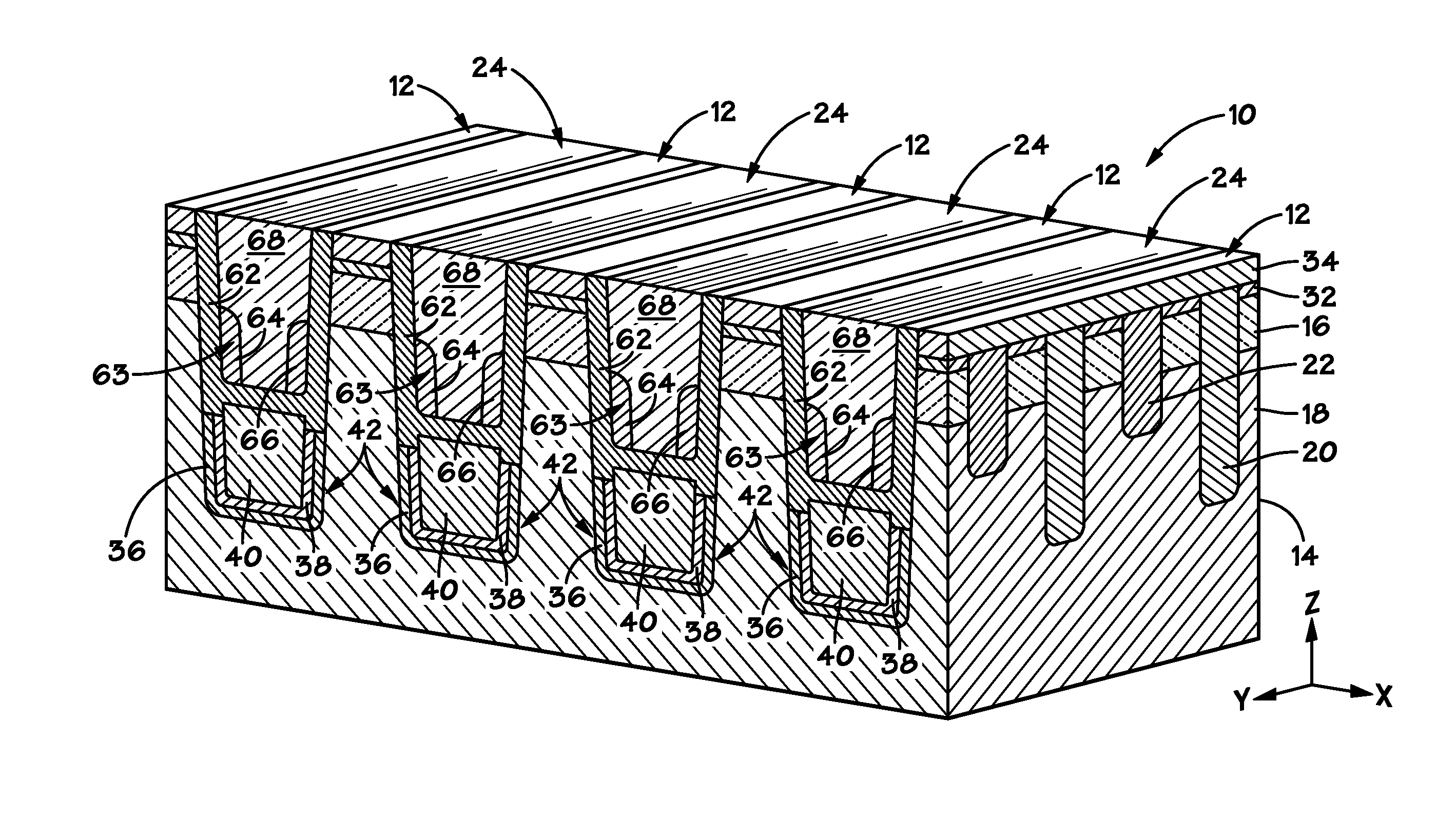
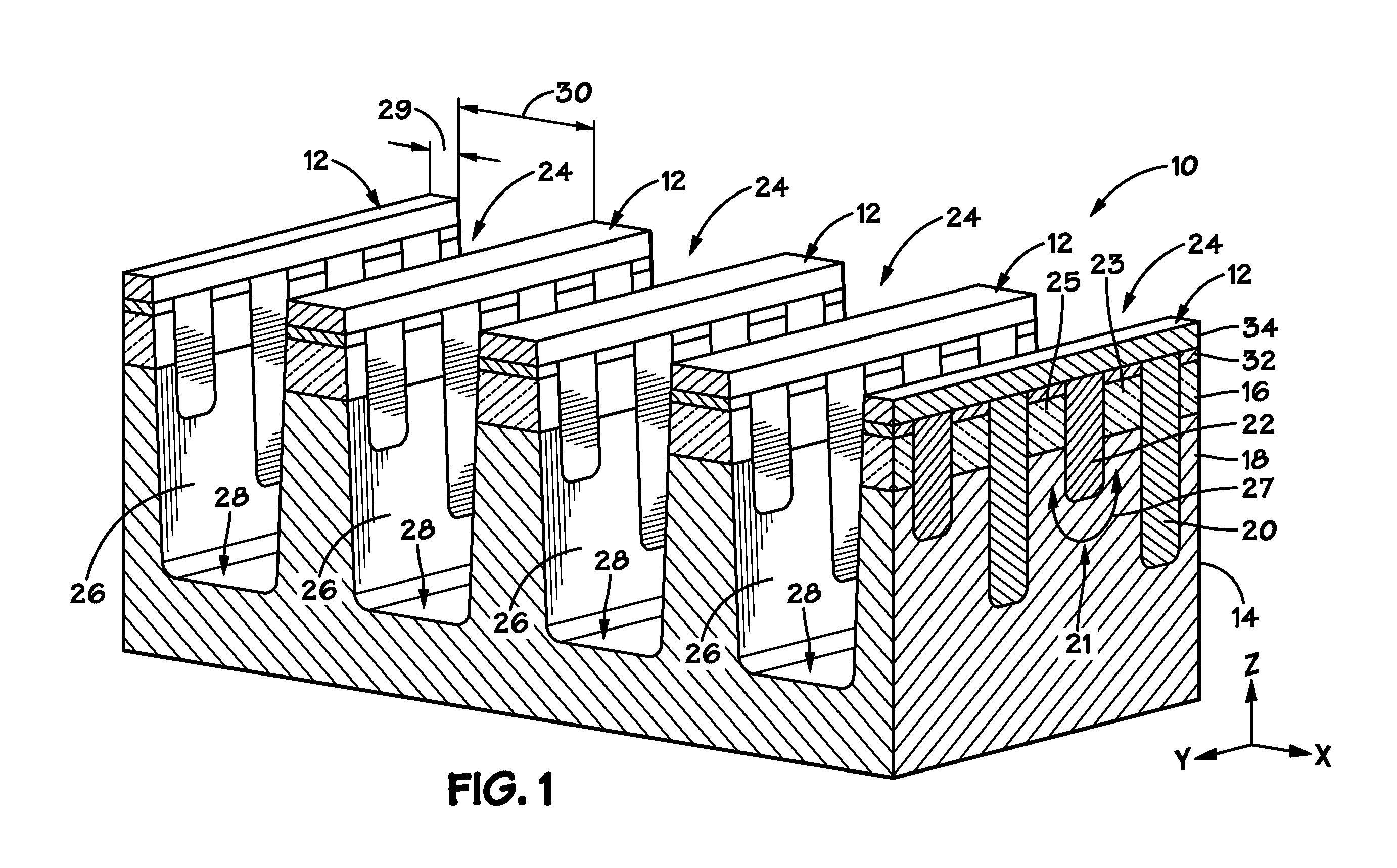
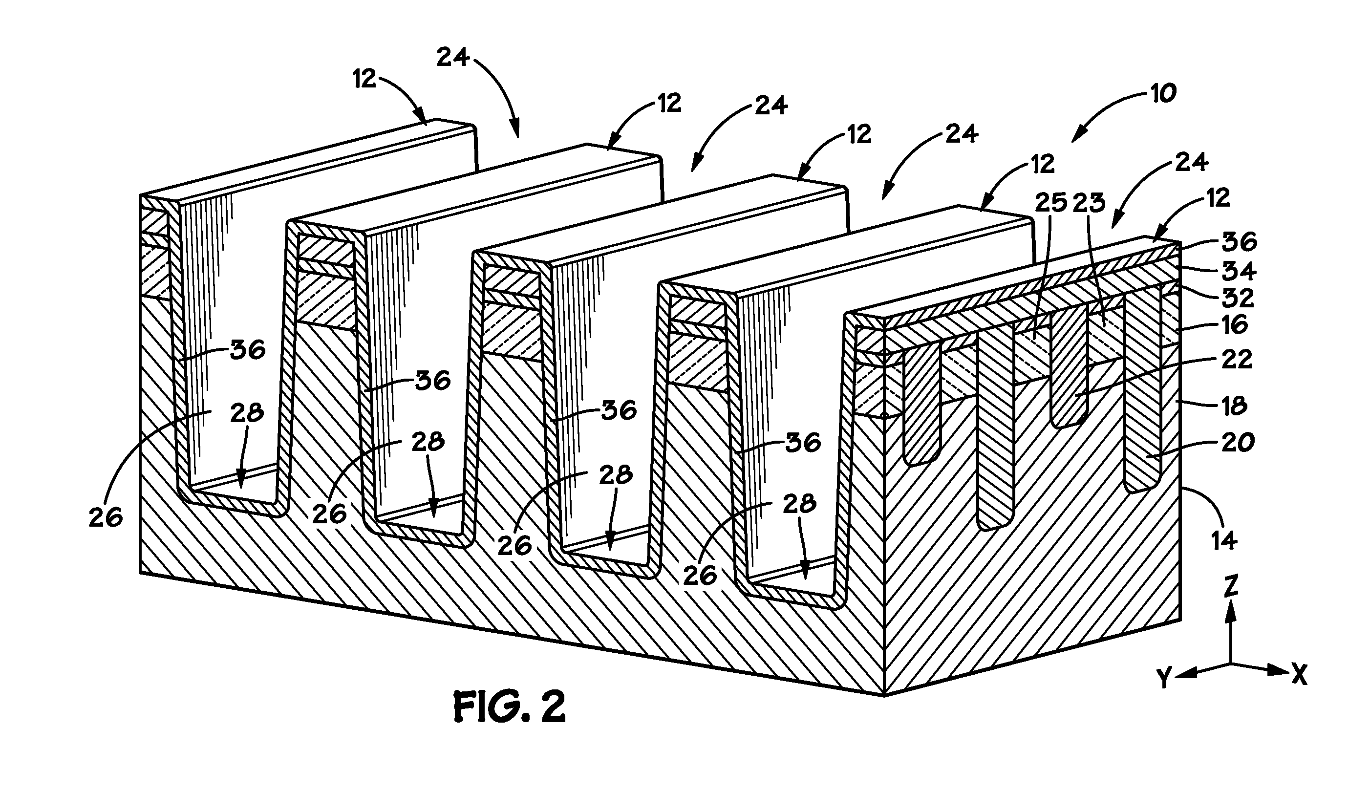
[0013]Some of the subsequently discussed embodiments may facilitate the manufacture of high aspect ratio structures such as finFETs having double gates for improved selection and operation. As is described in detail below, a highly resistive upper gate and a low resistive lower gate may be formed between each fin. The fin transistors may be operated by biasing the lower gate and upper gate, such that the lower gates provide preselection of a fin during biasing of the upper gates. The following discussion describes devices and process flows in accordance with embodiments of the present technique.

[0014]FIG. 1 depicts a cross-sectional plane view of a portion 10 of a memory array comprising high aspect ratio structures, e.g., fins 12, in accordance with an embodiment of the present invention. As used herein, the term “fin” refers to a tall, thin, semiconductor member extending from a substrate and generally having a length (i.e., y-direction) greater than the width (i.e., x-direction) ...


PUM


Abstract

A semiconductor device is provided that includes a fin having a first upper gate on a sidewall of the fin in a first trench and a second upper gate formed on the opposite sidewall of the fin. The device also includes a first lower gate on the sidewall and a second lower gate on the opposite sidewall, wherein the first upper gate is formed above the first lower gate and the second upper gate is formed above the second lower gate. Methods of manufacturing and operating the device are also included. A method of operation may include biasing the first upper gate and second upper gate to preselect the transistors of a fin and then biasing the first lower gate and second lower gate to operate the transistors of the fin.

Description

BACKGROUND[0001]1. Field of Invention[0002]Embodiments of the invention relate generally to electronic devices, and more specifically, to non-planar transistors and techniques for fabricating the same[0003]2. Description of Related Art[0004]This section is intended to introduce the reader to various aspects of art that may be related to various aspects of the present invention, which are described and / or claimed below. This discussion is believed to be helpful in providing the reader with background information to facilitate a better understanding of the various aspects of the present invention. Accordingly, it should be understood that these statements are to be read in this light, and not as admissions of prior art.[0005]Fin field effect transistors (finFETs) are often built around a fin (e.g., a tall, thin semiconductive member) extending generally perpendicularly from a substrate. Typically, a gate traverses the fin by conformally running up one side of the fin over the top and ...

Claims


Application Information

Patent Timeline
Patent Type & Authority Applications(United States)
IPC IPC(8): H01L29/78H03K17/00H01L21/28
CPCH01L27/10826H01L29/785H01L29/66795H01L27/10879H10B12/36H10B12/056
Inventor JUENGLING, WERNER
Owner MICRON TECH INC
Why Eureka
Try Eureka