In cell touch panel

Active Publication Date: 2012-05-24
HANNSTAR DISPLAY CORPORATION
View PDF4 Cites 3 Cited by
  • Summary
  • Abstract
  • Description
  • Claims
  • Application Information

AI Technical Summary

Benefits of technology

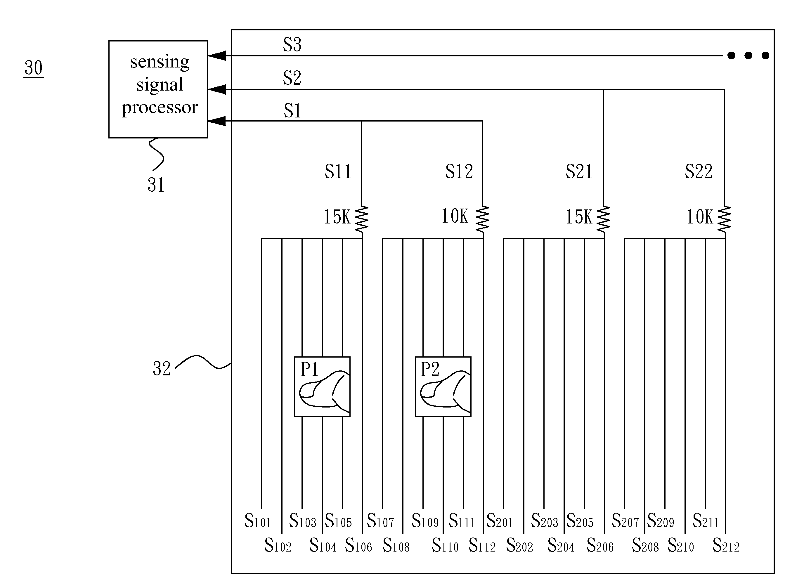
[0014]The embodiment employs resistance compensation to broaden voltage reading range of readout lines connected to a processing chip of an in cell

Problems solved by technology

The manufacturing processes of the resistance type of touch panel are simple; however, the additional touch panel may affect the optical performance and increase the manufacturing cost of the d

Method used


Image

  • In cell touch panel
  • In cell touch panel
  • In cell touch panel

Examples


Example

[0025]Reference will now be made in detail to specific embodiments of the invention. Examples of these embodiments are illustrated in accompanying drawings. While the invention will be described in conjunction with these specific embodiments, it will be understood that it is not intended to limit the invention to these embodiments. On the contrary, it is intended to cover alternatives, modifications, and equivalents as may be included within the spirit and scope of the invention as defined by the appended claims. In the following description, numerous specific details are set forth in order to provide a thorough understanding of the present invention. The present invention may be practiced without some or all of these specific details. In other instances, well-known process operations and components are not described in detail in order not to unnecessarily obscure the present invention. While drawings are illustrated in detail, it is appreciated that the quantity of the disclosed co...


PUM


Abstract

Embodiments of the present invention employ resistance compensation to broaden voltage reading range of readout lines connected to a processing chip of an in cell touch panel. The resolution of the in cell touch panel is increased under the condition that the number of pins of the processing chip is not increased or is unchanged.

Description

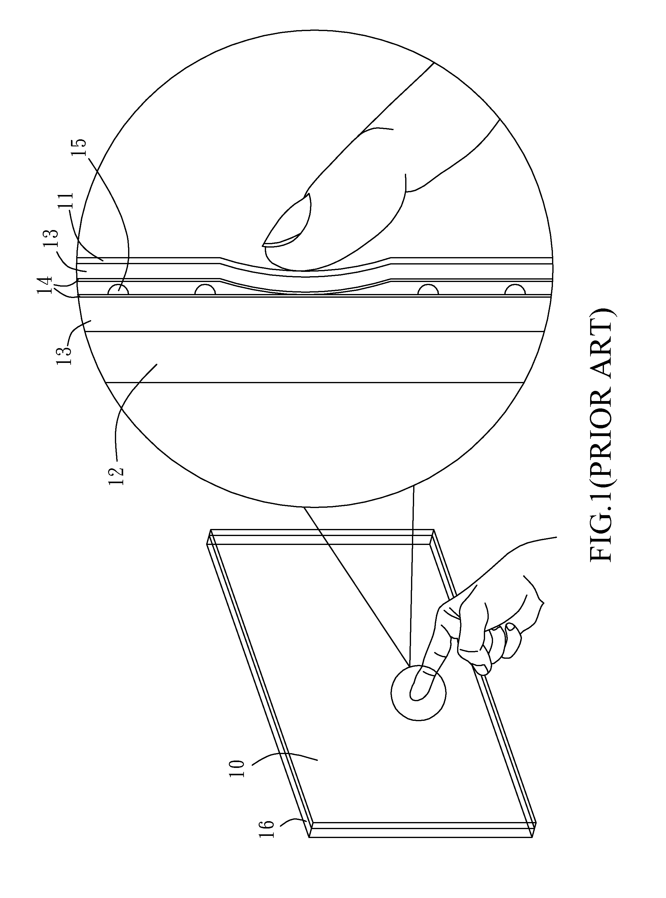
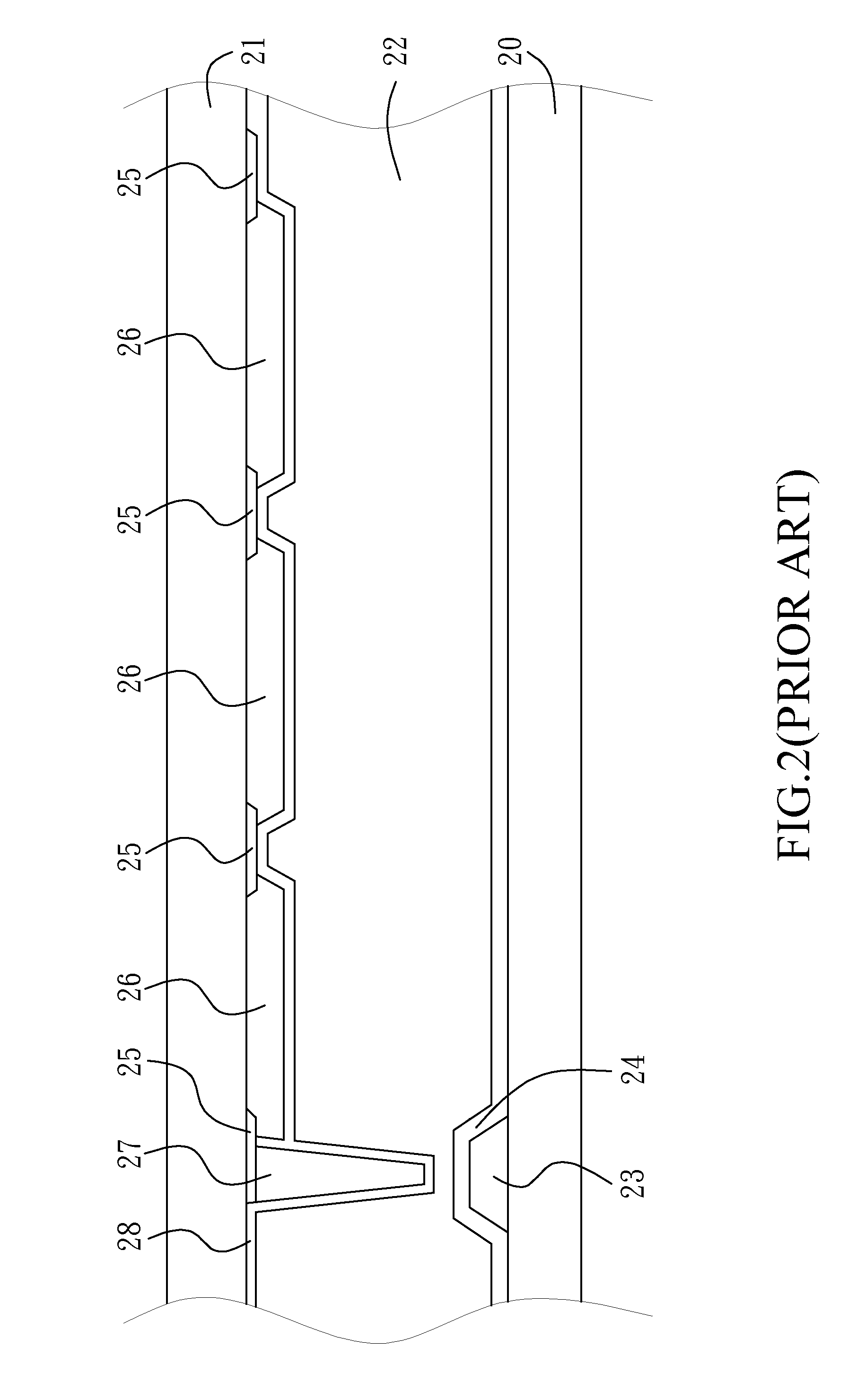
CROSS-REFERENCE TO RELATED APPLICATIONS[0001]The entire contents of Taiwan Patent Application No. 099140153, filed on Nov. 22, 2010, from which this application claims priority, are incorporated herein by reference.BACKGROUND OF THE INVENTION[0002]1. Field of the Invention[0003]The present invention relates to an in cell touch panel, more particularly, to an in cell touch panel with high resolution.[0004]2. Description of Related Art[0005]Displays with touch control functions are popularized nowadays. Typically a display realizes its touch control function by employing a touch panel whose working type may include resistance, capacitance, infrared ray, or surface acoustic wave.[0006]FIG. 1 illustrates a display 16 employing an additional resistance type of touch panel 10, which comprises a polymer substrate 11, a glass substrate 12, two conductive circuits 13 whose surface coated with indium tin oxide (ITO) 14 respectively arranged on the conductive circuit and between the two substr...

Claims


Application Information

Patent Timeline
IPC IPC(8): G06F3/042G06F3/044G06F3/045
CPCG06F3/0412G06F3/045G06F1/22G06F3/0416
Inventor JUAN, YI-CHUNGLIU, HSUAN-CHENLIN, SUNG-CHUNLIN, WEN-CHI
Owner HANNSTAR DISPLAY CORPORATION
Why Eureka
Try Eureka