
Electrically modulatable extended light source and a measurement device for characterizing a semiconductor including one such source

a measurement device and extended light source technology, applied in the direction of electronic circuit testing, vehicle components, lighting and heating apparatus, etc., can solve the problems of measurement technique and associated device unsuitable for volume lifetime measurement and inspection, device thus needs a relatively long measurement time, and takes several hours to draw, etc., to achieve simple operation mode and simple concept

Inactive Publication Date: 2012-05-31
UNIV PAUL CEZANNE
View PDF3 Cites 11 Cited by
  • Summary
  • Abstract
  • Description
  • Claims
  • Application Information

AI Technical Summary

Benefits of technology

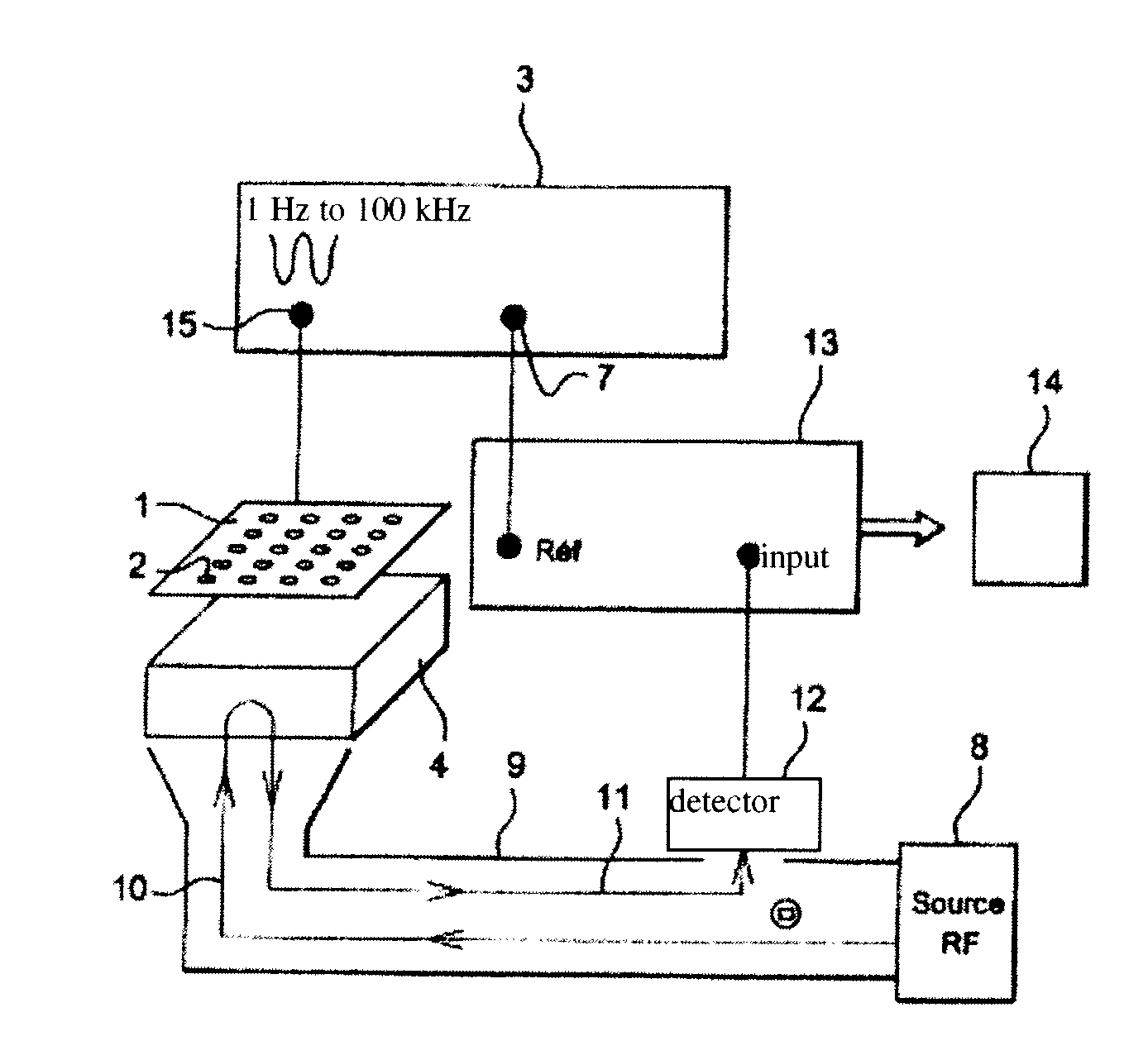
[0015]The aspect of the disclosed embodiments is to propose a light source of simple concept and simple operating mode, making possible global measurements on a specimen, in particular this source being combined with a measurement device makes it possible to determine, quickly and effectively on the production line, a volume lifetime τb and the rates of surface recombinations S of the minority carriers of a semiconductor wafer in the course of the manufacturing process for integrated circuits and photovoltaic cells, which lets one reveal, among other things, a possible metallic contamination through the measurement of the lifetime of the minority carriers.
[0016]In particular, this source should adapt itself to every type of material of the semiconductor wafer and it should illuminate in homogeneous fashion the entire surface of the wafer, regardless of its size, thus making possible global measurements and obtaining a mean value for the volume lifetime and the rate of recombination of the minority carriers in a single measurement.
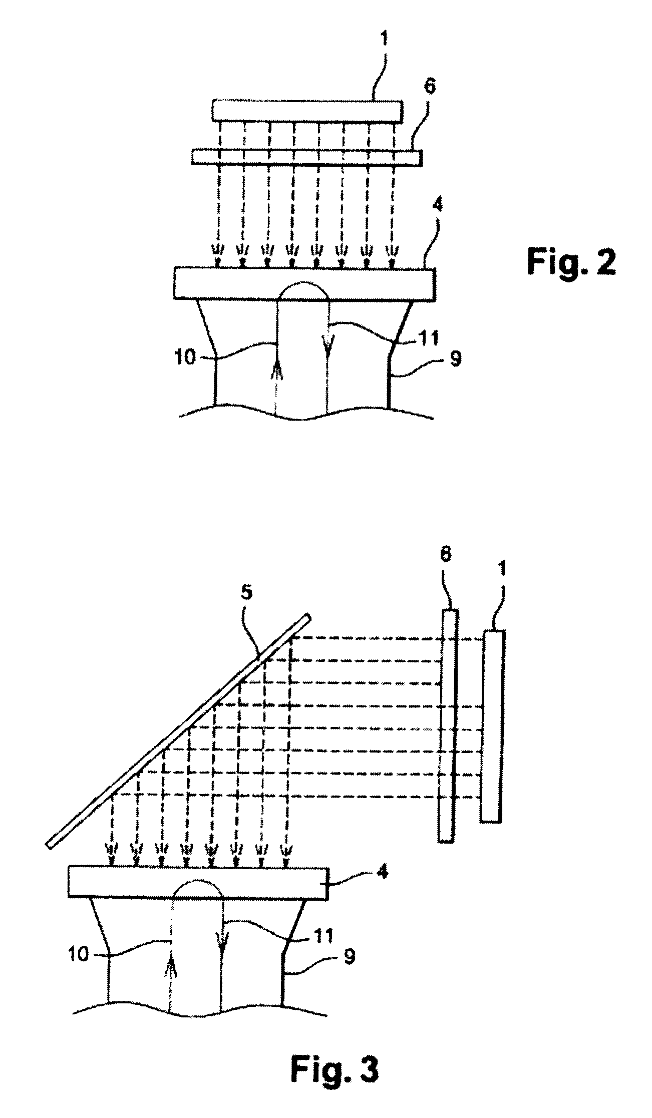
[0024]a neutral diffusion filter is preferably placed between the source and the surface of the object being illuminated to make the light beam emitted by the source more uniform.
[0028]a waveguide or an antenna making it possible to channel the waves emitted onto the nonilluminated surface of said semiconductor wafer and the waves reflected to a microwave detector, said waveguide or said antenna associated with said microwave detector being designed to pick up the signal produced by the waves reflected from said semiconductor wafer thus excited by said light source,

Problems solved by technology

This device thus needs a relatively long measurement time to obtain the data for the lifetime of the carriers for the entire wafer, generally it takes several hours to draw up the maps.
Therefore, this source makes the measurement technique and the associated device unsuited to measurements of volume lifetime and inspection for impurity contamination on the production line.

Method used


Image

  • Electrically modulatable extended light source and a measurement device for characterizing a semiconductor including one such source
  • Electrically modulatable extended light source and a measurement device for characterizing a semiconductor including one such source
  • Electrically modulatable extended light source and a measurement device for characterizing a semiconductor including one such source

Examples


Embodiment Construction

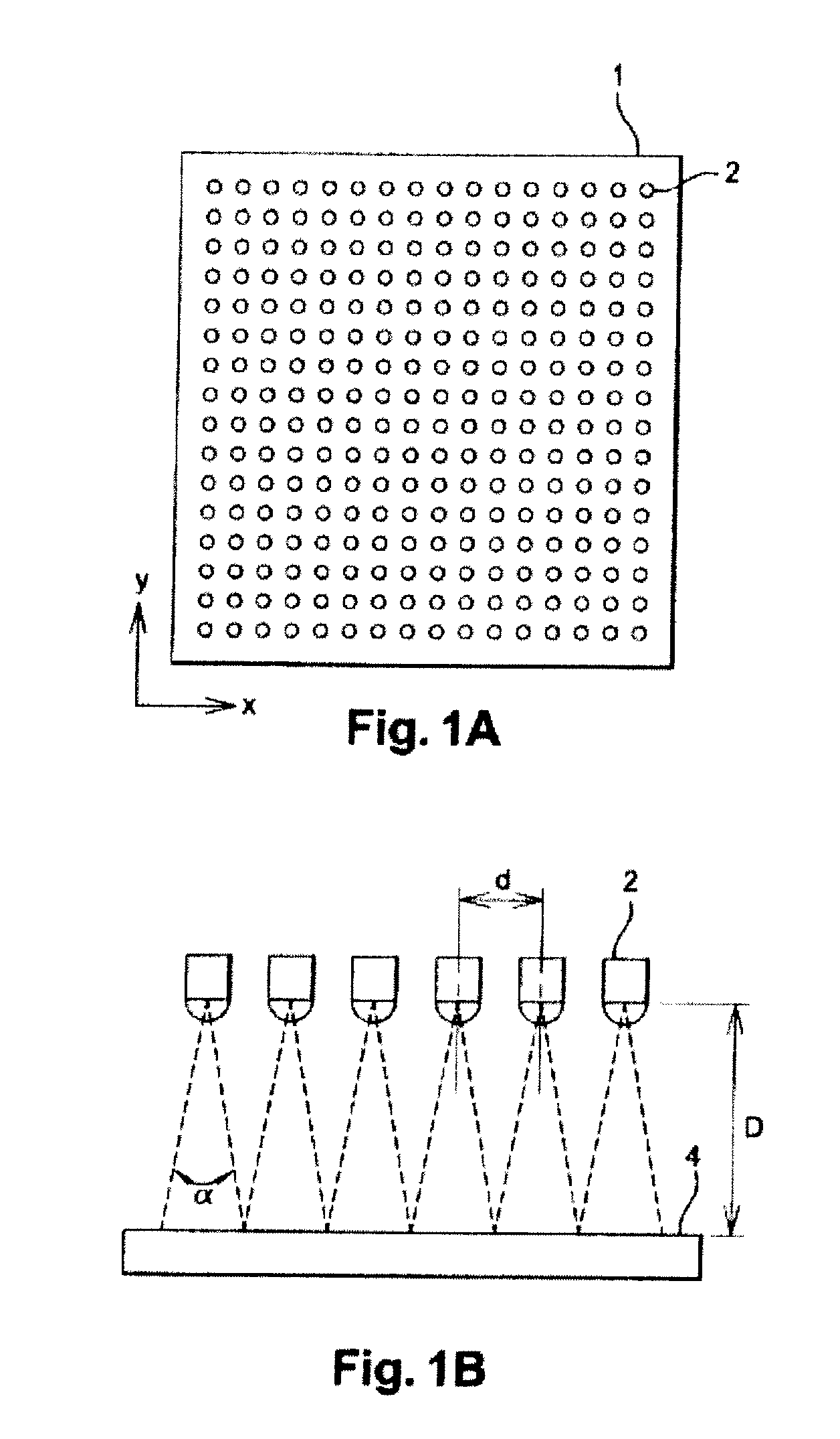
[0036]The disclosed embodiments concern a light source designed to inject excess carriers into a semiconductor wafer, thereby illuminating a surface of this semiconductor wafer in continuous and modulated fashion. FIG. 1.A shows a top view of one example of this light source, which has a rectangular geometry. The shape of the source can also be circular or oval.

[0037]The light source has a set of point sources 2 spaced at regular intervals in the X direction and in the Y direction, thus forming an array of point sources. All these point sources each emit a monochromatic beam and the same wave length, so that the overall source emits a monochromatic beam. The dimension of the beam emitted by the source 1 is at least equal to that of the surface being illuminated of the semiconductor wafer.

[0038]Advantageously, the distance (d) between two point sources and the distance (D) between the source and the surface being illuminated of the semiconductor wafer are chosen such that the monochr...


PUM


Abstract

A light source for injecting excess carriers into a semiconductor wafer, fully illuminating a surface of the wafer. According to the disclosed embodiments, the source includes at least one set of point sources which are spaced apart at regular intervals along the X and Y axes, such that the source emits a monochromatic beam of a size that is at least equal to that of the semiconductor wafer surface to be illuminated. Each of the point sources is sinusoidally modulated by a common electrical modulator, the distance between two point sources and the distance between the source and the semiconductor wafer surface to be illuminated being selected such that the monochromatic light beam uniformly illuminates the surface.

Description

CROSS REFERENCE TO RELATED APPLICATIONS[0001]This application is the National Stage of International Application No. PCT / EP2007 / 050950 International Filing Date, 31 Jan. 2007, which designated the United States of America, and which International Application was published under PCT Article 21 (2) as WO Publication No. WO2007 / 088176 and which claims priority from French Application No. 0650388, filed on 3 Feb. 2006, the disclosures of which are incorporated herein by reference in their entireties.BACKGROUND[0002]1. Field[0003]The disclosed embodiments concern an electrically modulable and extended light source designed to inject excess carriers into a semiconductor wafer, thereby illuminating it. In particular, this source, by having a measurement device, makes it possible to characterize electrical properties of this semiconductor wafer, such as the volume lifetime and the rate of surface recombination of the minority carriers of a semiconductor wafer. The disclosed embodiments appl...

Claims


Application Information

Patent Timeline
Patent Type & Authority Applications(United States)
IPC IPC(8): G01R31/265F21V5/04F21S4/00
CPCG01R31/311H01L22/00
Inventor PALAIS, OLIVIERPASQUINELLI, MARCEL
Owner UNIV PAUL CEZANNE
Learn More