
Group iii nitride semiconductor light-emitting device

a technology of nitride and semiconductor, which is applied in the manufacture of semiconductor/solid-state devices, semiconductor devices, electrical devices, etc., can solve the problems of poor crystallinity, failure to extract light to the outside, and scattering of light along the stripe on the sapphire substrate, etc., to achieve the effect of improving light extraction performan

Inactive Publication Date: 2012-05-31
TOYODA GOSEI CO LTD
View PDF1 Cites 20 Cited by
  • Summary
  • Abstract
  • Description
  • Claims
  • Application Information

AI Technical Summary

Benefits of technology

[0008]In view of the foregoing, an object of the present invention is to provide a method for producing a Group III nitride semiconductor light-emitting device comprising a substrate having a stripe-pattern embossment, and a layered structure formed on the substrate and including a Group III nitride semiconductor layer whose main surface is a non-polar plane or a semi-polar plane, which method realizes improvement of light extraction performance without causing deterioration of the crystallinity of the Group III nitride semiconductor layer.
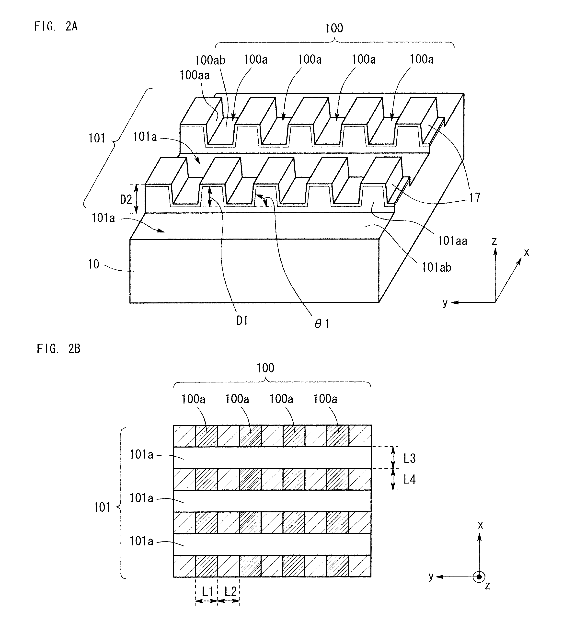
[0017]In the forming a second stripe-pattern embossment, the exposed portion of the sapphire substrate is dry-etched until the bottom surface of the thus-etched portion becomes flat. In this case, the bottom surface of the etched portion is not necessarily completely flat, and the flatness of the bottom surface may be of such a level that, in the subsequent forming of the Group III nitride semiconductor layer, crystal growth occurs dominantly on the exposed surface which is perpendicular to the main surface of the sapphire substrate. When a mesa of the sapphire substrate is dry-etched, as etching proceeds, edges of the mesa become rounded, and the height of the mesa decreases, resulting in gentle slope. In the forming a second stripe-pattern embossment, the bottom surface of the etched portion is made flat by utilizing this phenomenon.
[0019]The angle between the first direction and the second direction is preferably 30° to 150°, most preferably 90°, from the viewpoint of improvement of light extraction performance. Also, each of side surfaces of the first grooves is preferably inclined by 40° to 80° with respect to the main surface of the sapphire substrate, from the viewpoint of improvement of light extraction performance.
[0024]According to the method for producing a Group III nitride semiconductor light-emitting device of the present invention, light extraction performance can be improved without causing deterioration of the crystallinity of a Group III nitride semiconductor layer whose main surface is a non-polar plane or a semi-polar plane.

Problems solved by technology

However, when the embossment pattern formed on the sapphire substrate is a stripe pattern, since neither dents nor mesas are provided in the direction of the stripe, light propagated along the stripe on the sapphire substrate does not scatter and may fail to be extracted to the outside.
However, as described above, variation in crystal orientation may be increased, resulting in poor crystallinity.

Method used


Image

  • Group iii nitride semiconductor light-emitting device
  • Group iii nitride semiconductor light-emitting device
  • Group iii nitride semiconductor light-emitting device

Examples


embodiment 1

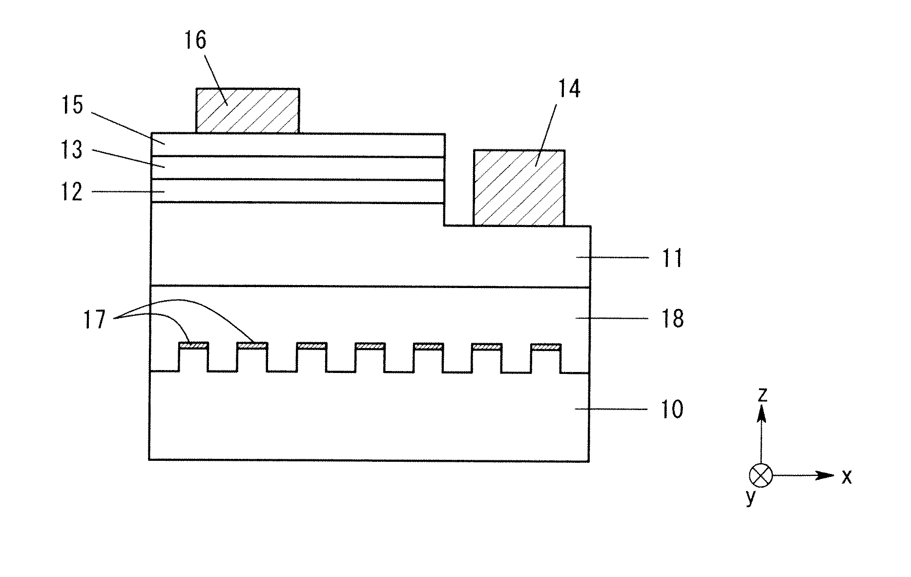
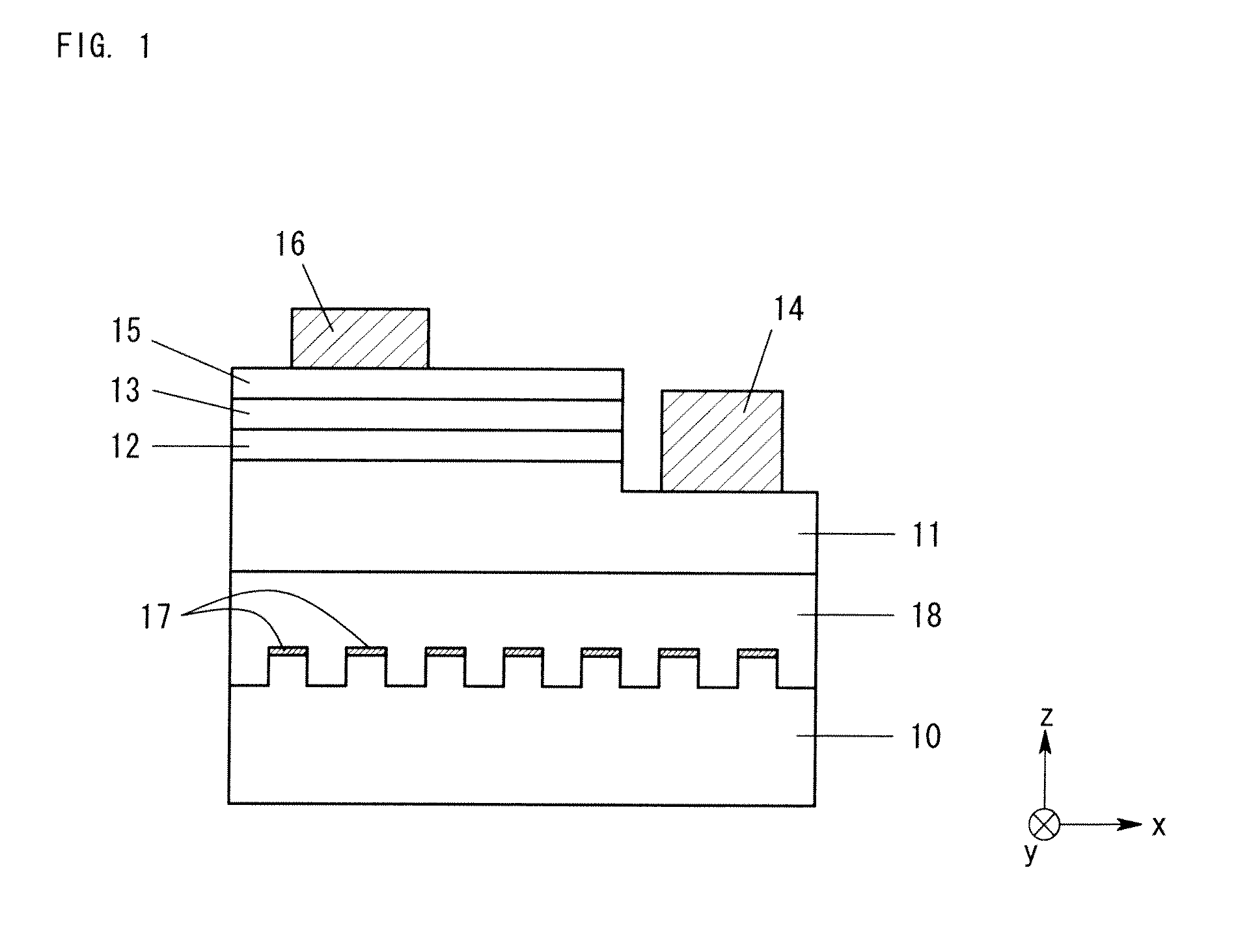
[0031]FIG. 1 shows the configuration of a Group III nitride semiconductor light-emitting device according to Embodiment 1. The Group III nitride semiconductor light-emitting device according to Embodiment 1 includes an embossed sapphire substrate 10 having an a-plane main surface; and a base layer 18, an n-type layer 11, a light-emitting layer 12, and a p-type layer 13, which are sequentially stacked on the embossed surface of the sapphire substrate 10 via a buffer layer (not illustrated), and each of which is formed of a Group III nitride semiconductor layer whose main surface is m-plane. The layered structure of the present invention corresponds to a structure including the n-type layer 11, the light-emitting layer 12, and the p-type layer 13. A portion of the light-emitting layer 12 and a portion of the p-type layer 13 are removed, and the corresponding portion of the n-type layer 11 is exposed. An n-electrode 14 is formed on the exposed portion of the n-type layer 11. An ITO tra...


PUM


Abstract

A method for producing a Group III nitride semiconductor light-emitting device includes forming a first stripe-pattern embossment on the top surface of a sapphire substrate, so that first grooves parallel to the x-axis direction (the c-axis direction of the sapphire substrate) are periodically arranged at specific intervals. Subsequently, an insulating film is formed over the entire surface of the first stripe-pattern embossment. Next, a second stripe-pattern embossment is formed so that second grooves, each having a flat bottom surface, are periodically arranged at specific intervals and parallel to the y-axis direction, which is orthogonal to the x-axis direction. A GaN crystal is grown through MOCVD on side surfaces of each second groove of the sapphire substrate, to thereby form, on the sapphire substrate, an m-plane GaN base layer. An LED device structure is formed on the base layer, to thereby produce a light-emitting device.

Description

BACKGROUND OF THE INVENTION[0001]1. Field of the Invention[0002]The present invention relates to a method for producing a Group III nitride semiconductor light-emitting device whose main surface is a plane other than c-plane, which method realizes improvement of light extraction performance without causing deterioration of crystallinity.[0003]2. Background Art[0004]Patent document 1 discloses a method for producing a GaN crystal layer whose main surface is a non-polar plane (e.g., m-plane or a-plane) or a semi-polar plane (e.g., (11-22) plane) by growing GaN crystal on side surfaces of dents or mesas of an embossed sapphire substrate. Recently, there has been actively developed a Group III nitride semiconductor light-emitting device whose main surface is such a non-polar or semi-polar plane, since such a device is expected to exhibit improved internal quantum efficiency by virtue of increased recombination of electrons and holes resulting from a small internal electric field. In suc...

Claims


Application Information

Patent Timeline
Patent Type & Authority Applications(United States)
IPC IPC(8): H01L33/02
CPCH01L21/0242H01L21/02458H01L21/0254H01L21/02609H01L33/20H01L21/02642H01L33/007H01L33/16H01L21/02639
Inventor OKUNO, KOJI
Owner TOYODA GOSEI CO LTD
Learn More