
Group iii nitride semiconductor light-emitting device

a technology of nitride and semiconductor, applied in the direction of semiconductor devices, basic electric elements, electrical equipment, etc., can solve the problem of no suggestion that light extraction performance is improved, and achieve the effect of increasing the external quantum efficiency of the light-emitting devi

Active Publication Date: 2012-10-04
TOYODA GOSEI CO LTD
View PDF7 Cites 7 Cited by
  • Summary
  • Abstract
  • Description
  • Claims
  • Application Information

AI Technical Summary

Benefits of technology

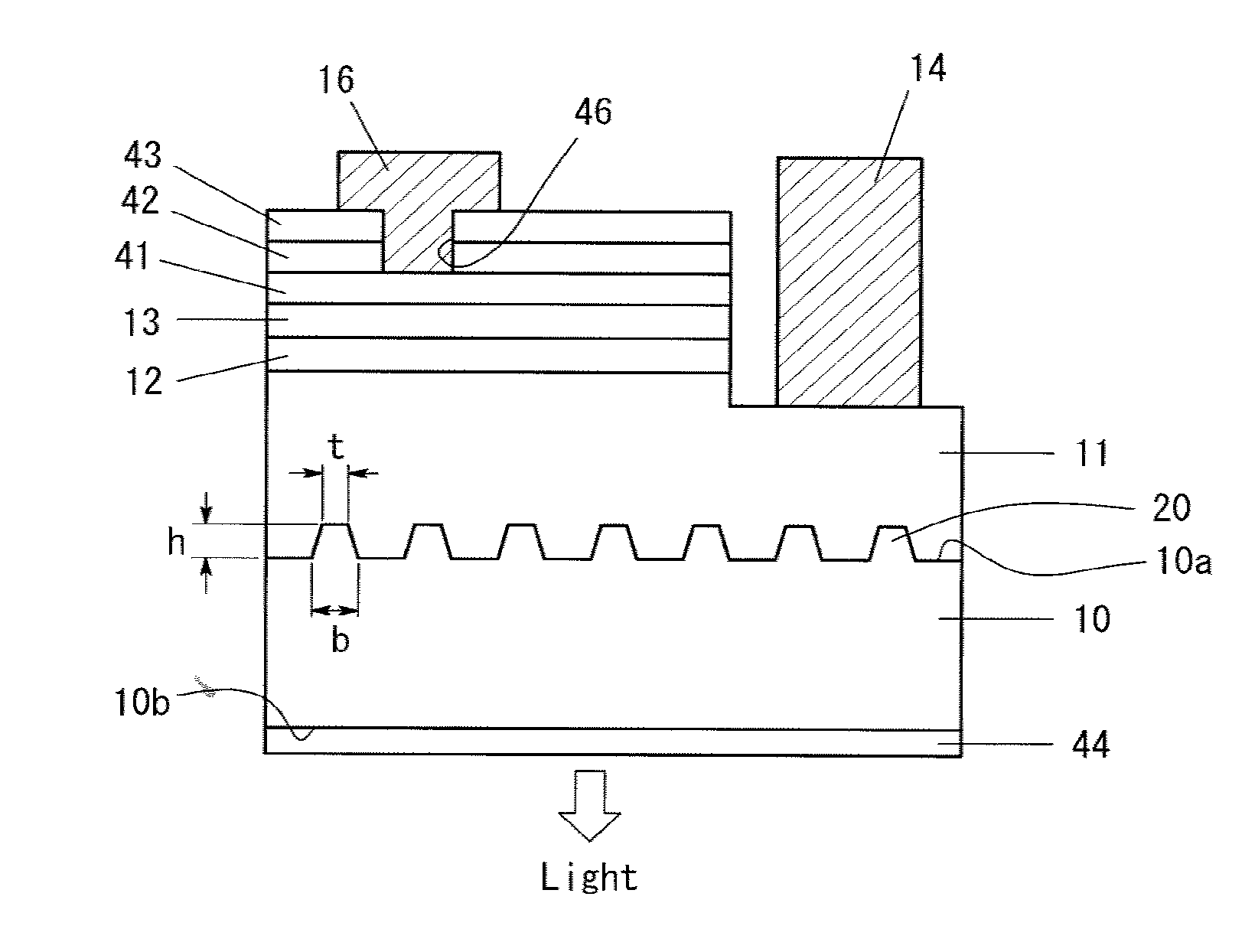
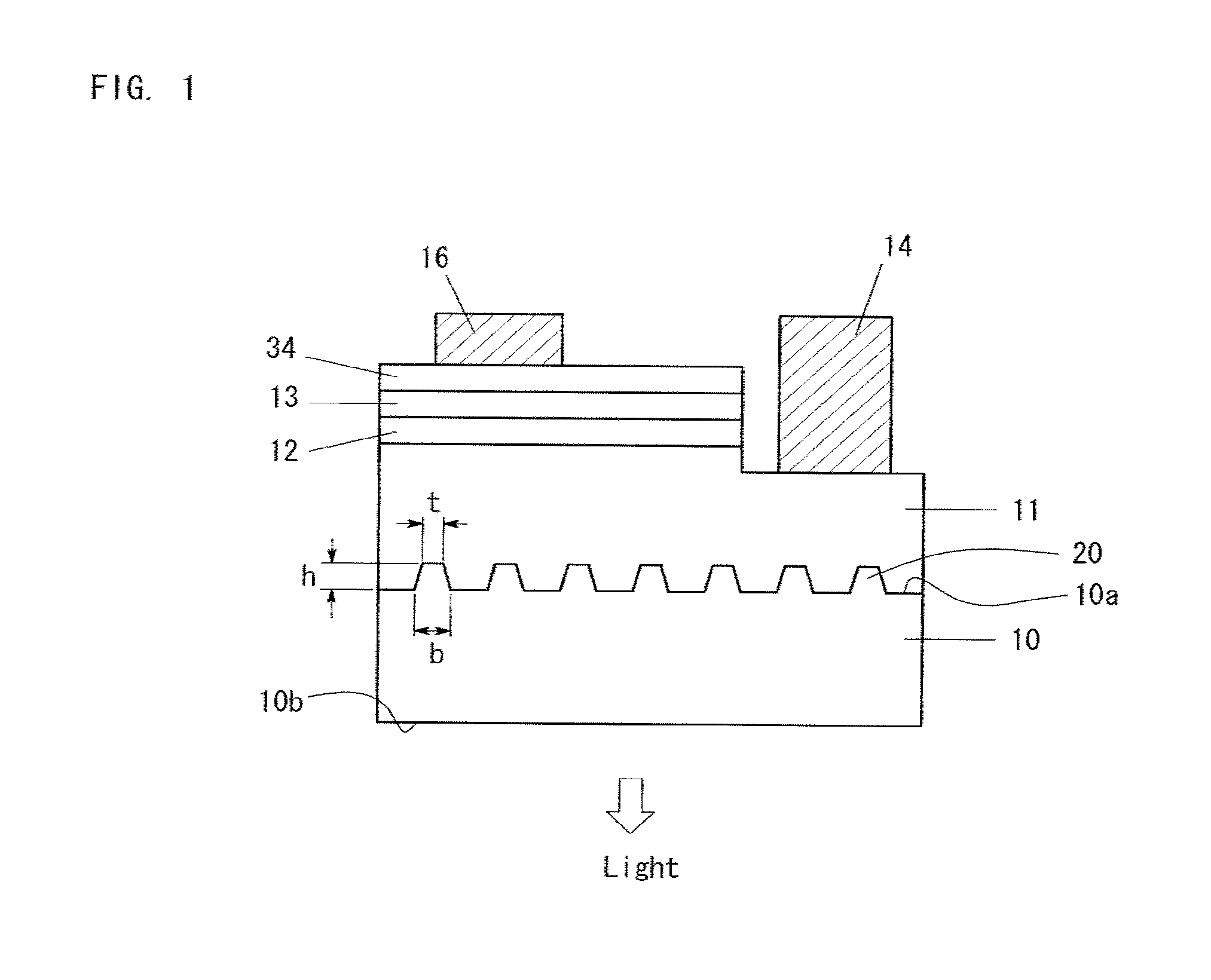
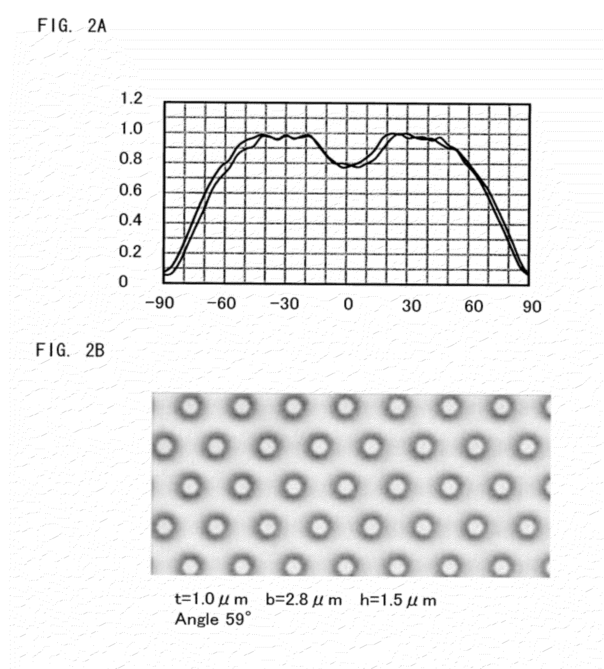
[0010]In the present invention, a light interference pattern is generated by forming a periodic structure of at least one of dents and mesas on the sapphire substrate with a period of a wavelength order of the light emitted from the light-emitting layer. Thus, a high-intensity light output can be obtained in a direction making a predetermined angle with respect to a normal to the sapphire substrate. This allows the improvement of the light extraction performance of the light-emitting device. This periodic structure may be a two-dimensional periodic structure in a direction of two axes at right angles to each other on the sapphire substrate or a periodic structure which is point symmetrical with respect to the center on the sapphire substrate. It may be a two-dimensional periodic lattice structure such as regular polygon including equilateral triangle or regular hexagon, or polygon. Additionally, a two-dimensional array means an array that is periodic in a biaxial direction on a surface. A two-dimensional periodic structure means a structure that is periodic in a biaxial direction.
[0012]The period of the periodic structure is preferably 4 μm or less. When the period is 4 μm or less, a light interference pattern is generated. When the period exceeds 4 μm, a light interference pattern is difficult to generate. Therefore, the period is preferably 4 μm or less. The light interference pattern varies with period. This can increase the light emission at a desired angle with respect to a normal to the sapphire substrate.
[0015]A transparent film may be formed on a light output surface of the Group III nitride semiconductor light-emitting device; and the film has a transmittance distribution that the light transmittance increases in a position where the light intensity is high in the interference pattern appeared on the light output surface. In the interference pattern, it can be considered that the light energy is focused on a portion where the light intensity increases. Therefore, light extraction performance can be improved in a direction where the light intensity increases by forming a transparent film which transmits more light in that direction. The total light output in all directions also increases because the light focused in that direction can be more effectively output to the outside.
[0016]Preferably, a light reflecting film may be formed on a light reflecting surface opposite to the light output surface of the Group III nitride semiconductor light-emitting device; and the film has a reflectance distribution that the light reflectance increases in a position where the light intensity is high in the interference pattern appeared on the light reflecting surface. In this case, as is the case with the above, the light is focused in a direction where the light intensity increases. Therefore, light extraction performance can be improved by forming a light reflecting film which effectively reflects more light in that direction on the light extracting surface side.
[0018]According to the present invention, a high-intensity light output can be obtained at a desired angle with respect to a normal to the sapphire substrate by forming a periodic structure of dents or mesas arranged in a two-dimensional array with a period which generates a light intensity interference pattern for the light emitted from a light-emitting layer, on the surface on the sapphire substrate surface where a layered structure is provided. Since the light is focused on a region where the interference intensity of the interference pattern is high, the total light output in all directions also increases as well as the light can be output in a specific direction. This results in the increase in the external quantum efficiency of the light-emitting device.

Problems solved by technology

Moreover, there is no suggestion that light extraction performance is improved using the light interference pattern.

Method used


Image

  • Group iii nitride semiconductor light-emitting device
  • Group iii nitride semiconductor light-emitting device
  • Group iii nitride semiconductor light-emitting device

Examples


embodiment 1

[0047]FIG. 1 is a cross-sectional view showing the configuration of a Group III nitride semiconductor light-emitting device according to Embodiment 1. The Group III nitride semiconductor light-emitting device according to Embodiment 1 includes a sapphire substrate 10 having a two-dimensional periodic structure of mesas 20 on a surface thereof. And the device includes an n-type layer 11, a light-emitting layer 12, and a p-type layer 13, which are sequentially deposited on the surface of the sapphire substrate 10 and the surface of the two-dimensional periodic structure via a buffer layer (not illustrated), and each of which is formed of a Group III nitride semiconductor. The layered structure of the present invention corresponds to a structure including the n-type layer 11, the light-emitting layer 12, and the p-type layer 13. A portion of the light-emitting layer 12 and a portion of the p-type layer 13 are removed by etching, and the corresponding portion of the surface of the n-typ...

embodiment 2

[0067]FIG. 10 shows the configuration of a light-emitting device according to Embodiment 2 utilizing a light intensity interference pattern. A multilayer transparent film 33 comprising a plurality of layers with a different refractive index was formed on the light output surface 10b of the sapphire substrate 10 in the light-emitting device according to Embodiment 1. The multilayer transparent film 33 is designed to have a thickness of each layer so that more light is transmitted at an angle where the light intensity increases in the light intensity distribution (interference pattern) of the light transmitted through the two-dimensional periodic structure of mesas 20. By this thickness design, the interference pattern of the transmitted light through the multilayer transparent film 33 can be the same as that of the emitted light from the two-dimensional periodic structure of mesas 20. Thus, the light in a direction where the light intensity increases in the light intensity distributi...

embodiment 3

[0068]As shown in FIG. 11, the present embodiment comprises a multilayer reflecting film (DBR) 35 between the reflecting film 34 also serving as an electrode and the p-type layer 13 in the light-emitting device according to Embodiment 1. The multilayer reflecting film 35 also comprises a plurality of dielectric layers with a different refractive index deposited in the same way as the multilayer transparent film 33 of Embodiment 2. The light which is emitted from the light-emitting layer 12 to the multilayer reflecting film 35 is reflected to the light output surface 10b by the multilayer reflecting film 35. The light which is emitted from the light-emitting layer 12 to the periodic structure of mesas 20 is reflected to the multilayer reflecting film 35 by the periodic structure. And the light which incidents to the multilayer reflecting film 35 is reflected to the periodic structure of mesas 20 by the multilayer reflecting film 35. The multilayer reflecting film 35 is designed to ha...


PUM


Abstract

The present invention provides a Group III nitride semiconductor light-emitting device exhibiting high-intensity light output in a specific direction and improved light extraction performance. The Group III nitride semiconductor light-emitting device comprises a sapphire substrate, and a layered structure having a light-emitting layer provided on the sapphire substrate and formed of a Group III nitride semiconductor. On the surface on the layered structure side of the sapphire substrate, a two-dimensional periodic structure of mesas is formed with a period which generates a light intensity interference pattern for the light emitted from the light-emitting layer. The light reflected by or transmitted through the two-dimensional periodic structure has an interference pattern. Therefore, the light focused on a region where the light intensity is high in the interference pattern can be effectively output to the outside, resulting in the improvement of light extraction performance as well as the achievement of desired directional characteristics.

Description

BACKGROUND OF THE INVENTION[0001]1. Field of the Invention[0002]The present invention relates to a Group III nitride semiconductor light-emitting device whose light extraction performance is improved by forming irregularities on a sapphire substrate included in the device.[0003]2. Background Art[0004]In recent years, Group III nitride semiconductor light-emitting devices have begun to be used in general illumination applications, and have been strongly required to exhibit improved light extraction performance. Japanese Patent Application Laid-Open (kokai) No. 2003-318441 discloses a method for improving the light extraction performance of a semiconductor light-emitting device, in which irregularities are formed on a sapphire substrate. In the case of a semiconductor light-emitting device including a flat sapphire substrate having no irregularities, light propagated in the device in a direction horizontal to the substrate is confined in semiconductor layers and is attenuated through,...

Claims


Application Information

Patent Timeline
IPC IPC(8): H01L33/06
CPCH01L33/20H01L2933/0083H01L33/46H01L33/42
Inventor YAHATA, KOSUKENAKAJO, NAOKIGOSHONOO, KOICHIISHIGURO, YUYA
Owner TOYODA GOSEI CO LTD
Learn More