Method for cutting liquid crystal panel

a technology cutting method, which is applied in the direction of manufacturing tools, instruments, transportation and packaging, etc., can solve the problems of limited use of liquid crystal display panel for various purposes, and cut liquid crystal display panel

Inactive Publication Date: 2012-06-07
TOVIS
View PDF13 Cites 7 Cited by
  • Summary
  • Abstract
  • Description
  • Claims
  • Application Information

AI Technical Summary

Benefits of technology

[0014]According to the present invention, since an external force is applied in a direction to urge the lower panel to be bent toward an outer surface thereof to break the upper panel and the lower panel after forming scribe lines on the same, an alignment layer of the lower panel within a viewing area of a liquid crystal display panel which will be obtained by cutting can be prevented from being damaged by the deformation of the spacer which is interposed between the upper panel and the lower panel.

Problems solved by technology

Generally, a liquid crystal display panel has one of some standardized sizes, so use of the liquid crystal panel for various purposes is limited by the standardized size.
An alignment layer of a viewing area of a lower panel near the spacer can be damaged by the momentary deformation of the spacer, and damage of the alignment layer may cause light leakage problem and this may result in an error in the cut liquid crystal display panel.

Method used


Image

  • Method for cutting liquid crystal panel
  • Method for cutting liquid crystal panel
  • Method for cutting liquid crystal panel

Examples


Embodiment Construction

[0020]The present invention will now be described more fully hereinafter with reference to the accompanying drawings, in which preferred embodiments of the invention are shown.

[0021]In the drawings, the thickness of layers, films, panels, regions, etc. are exaggerated for clarity. Like reference numerals designate like elements throughout the specification. It will be understood that when an element such as a layer, film, region or substrate is referred to as being “on” another element, it can be directly on the other element or intervening elements may also be present. In contrast, when an element is referred to as being “directly on” another element, there are no intervening elements present.

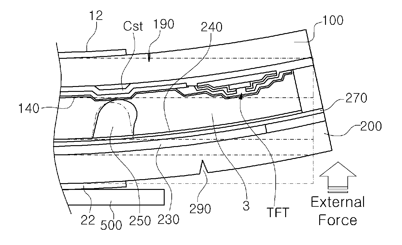
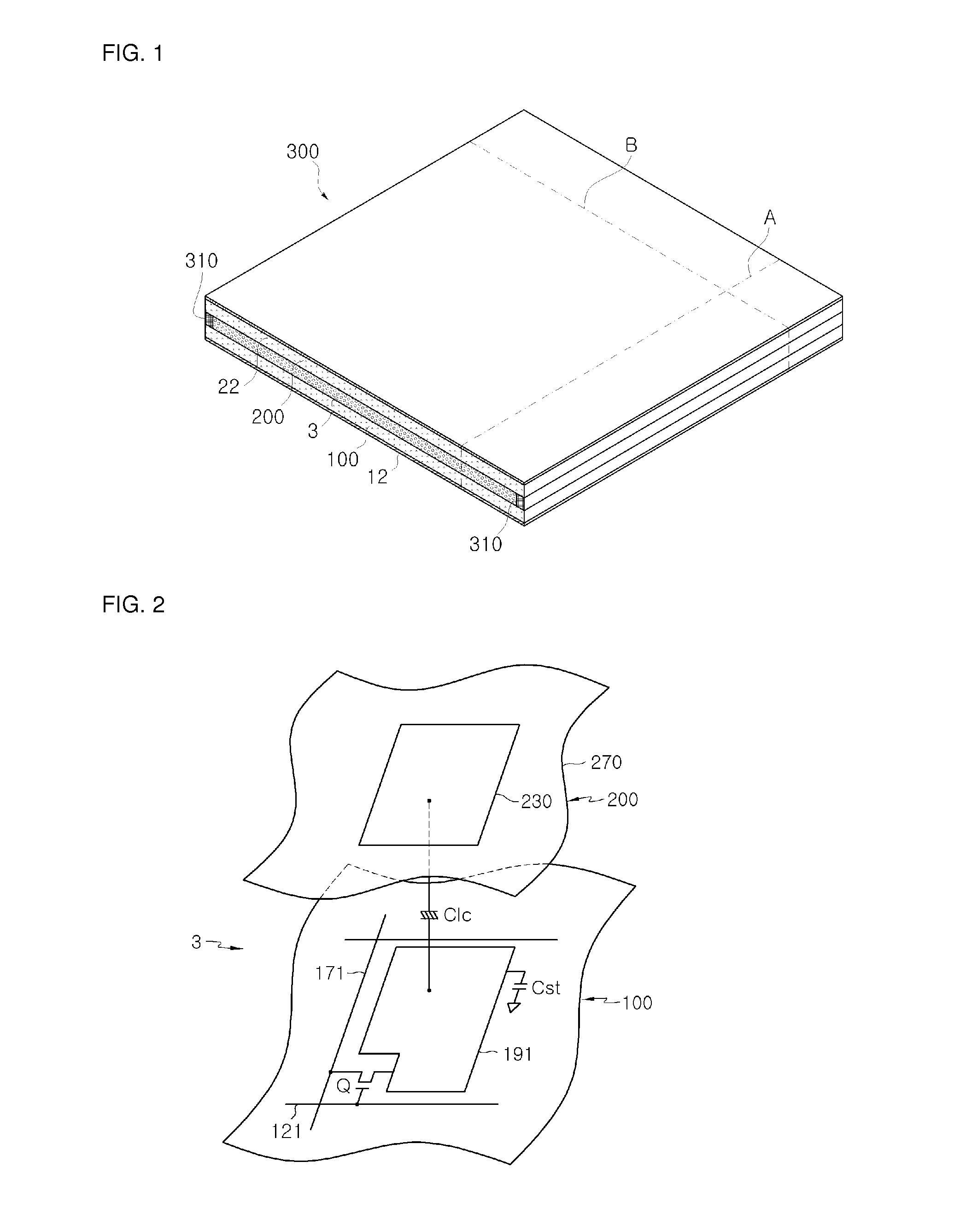
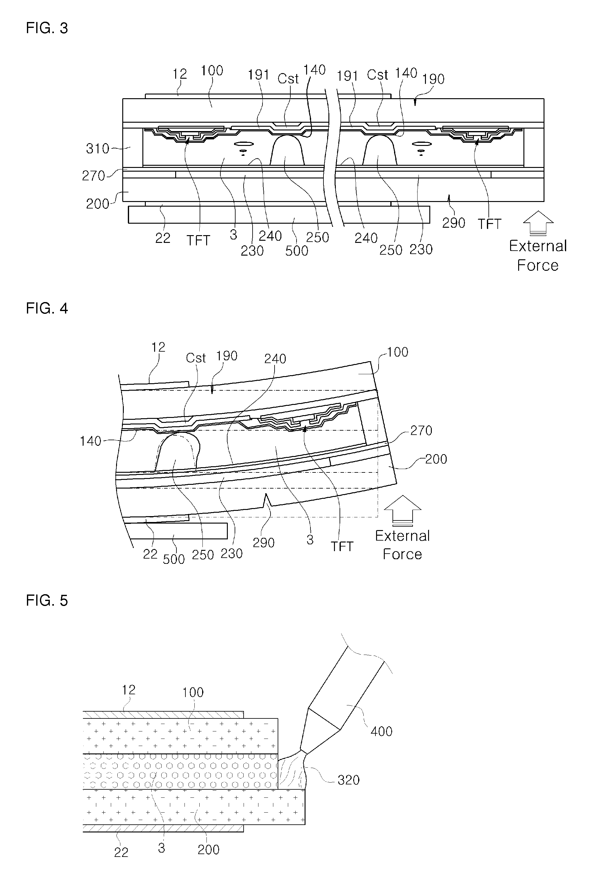
[0022]Referring to FIG. 1 to FIG. 3, liquid crystal panel assembly 300 to which a cutting method according to an embodiment of the present invention includes lower and upper panels 100 and 200 which face each other, and a liquid crystal layer 3 which is interposed between panels 100 and 200 an...


PUM

PropertyMeasurementUnit
external forceaaaaaaaaaa
dielectric anisotropyaaaaaaaaaa
transmittanceaaaaaaaaaa

Abstract

The present invention relates to a method for cutting a liquid crystal display panel. A method for cutting a liquid crystal display panel which includes an upper panel and a lower panel includes: forming scribe lines on the upper panel and the lower panel respectively along a cutting direction; and breaking the upper panel and the lower panel by applying an external force at an outside of the scribe lines in a direction to urge the lower panel to be bent toward an outer surface thereof.

Description

CROSS-REFERENCE TO RELATED APPLICATION[0001]This application claims priority to and the benefit of Korean Patent Application No. 10-2009-0053476 filed in the Korean Intellectual Property Office on Jun. 16, 2009, the entire contents of which are incorporated herein by reference.FIELD OF THE INVENTION [0002]The present invention relates to a method for cutting a liquid crystal display panel.BACKGROUND ART [0003]Generally, a liquid crystal display (LCD) includes two display panels and a liquid crystal layer disposed therebetween and having a dielectric anisotropy. An electric filed is formed in the liquid crystal layer, and a transmittance of light passing the liquid crystal layer is regulated by regulating amplitude of the electric field so as to obtain a desired image. Such a liquid crystal display is representative one of a flat panel display (FPD), and TFT-LCD which uses thin film transistor (TFT) as a switching element is widely used.[0004]A plurality of display signal lines i.e.,...

Claims


Application Information

Patent Timeline
Patent Type & Authority Applications(United States)
IPC IPC(8): B26F3/00C03B33/02
CPCB26D3/06B26F3/002G02F2001/13398C03B33/076G02F1/133351C03B33/033G02F1/13398Y10T225/12C03B23/22C03B33/02G02F1/13
Inventor KIM, YONG BEOMKIM, DONG HYUN
Owner TOVIS
Why Eureka
Try Eureka