Biscarbazole derivative, material for organic electroluminescence device and organic electroluminescence device using the same

a technology of organic electroluminescence and derivatives, applied in the field of biscarbazole derivatives, can solve the problems of insufficient capability, unfavorable luminescence properties, and inability to obtain favorable luminescence properties and lifetime properties, and achieve excellent carrier balance

Active Publication Date: 2012-06-07
IDEMITSU KOSAN CO LTD
View PDF3 Cites 25 Cited by
  • Summary
  • Abstract
  • Description
  • Claims
  • Application Information

AI Technical Summary

Benefits of technology

[0016]Accordingly, an object of the invention is to provide a novel biscarbazole derivative having a hole transporting capability and an electron transporting capability and exhibiting an excellent carrier balance, a material for an organic EL device (hereinafter, referred to as an organic-EL-device material) and a phosphorescent and long-life organic EL device using those.

Problems solved by technology

The compound I has only a single carbazole skeleton and lacks a hole transporting capability, so that a favorable luminescence property cannot be obtained.
Accordingly, an overlapping margin of the carbazole skeleton between molecules is impaired, so that a hole transporting capability is insufficient and a re-bonding position of charges is likely to be closer to the anode.
Consequently, favorable luminescence property and lifetime property cannot be obtained.
However, since none of the compounds III to VI has an electron-deficient nitrogen-containing hetero aromatic ring structure, adjustment of carrier balance between holes and electrons is difficult, so that a favorable luminescence property cannot be obtained.
Accordingly, the overlapping margin between the molecules becomes small and a hole transporting capability becomes insufficient, so that favorable luminescence property and lifetime property cannot be obtained.
However, since the compound is considered to exhibit a high electron transporting capability, when used as a host material, the compound provides a poor carrier balance within the emitting layer and fails to exhibit a favorable luminescence property.

Method used


Image

  • Biscarbazole derivative, material for organic electroluminescence device and organic electroluminescence device using the same
  • Biscarbazole derivative, material for organic electroluminescence device and organic electroluminescence device using the same
  • Biscarbazole derivative, material for organic electroluminescence device and organic electroluminescence device using the same

Examples


first exemplary embodiment

Arrangement of Organic EL Device

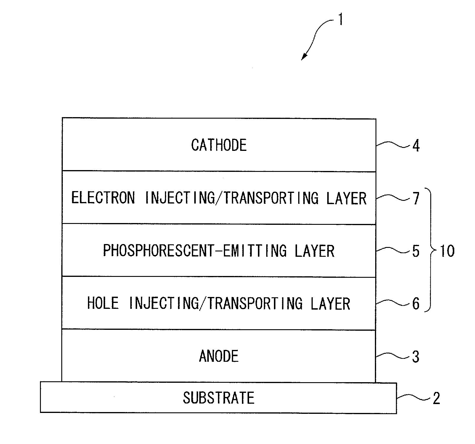
[0093]First of all, arrangement(s) of an organic EL device will be described below.

[0094]The followings are representative arrangement examples of an organic EL device:

(1) anode / emitting layer / cathode;

(2) anode / hole injecting layer / emitting layer / cathode;

(3) anode / emitting layer / electron injecting•transporting layer / cathode;

(4) anode / hole injecting layer / emitting layer / electron injecting•transporting layer / cathode;

(5) anode / organic semiconductor layer / emitting layer / cathode;

(6) anode / organic semiconductor layer / electron blocking layer / emitting layer / cathode;

(7) anode / organic semiconductor layer / emitting layer / adhesion improving layer / cathode;

(8) anode / hole injecting•transporting layer / emitting layer / electron injecting•transporting layer / cathode;

(9) anode / insulating layer / emitting layer / insulating layer / cathode;

(10) anode / inorganic semiconductor layer / insulating layer / emitting layer / insulating layer / cathode;

(11) anode / organic semiconductor layer / insula...

second exemplary embodiment

[0239]Next, an organic EL device according to a second exemplary embodiment will be described below.

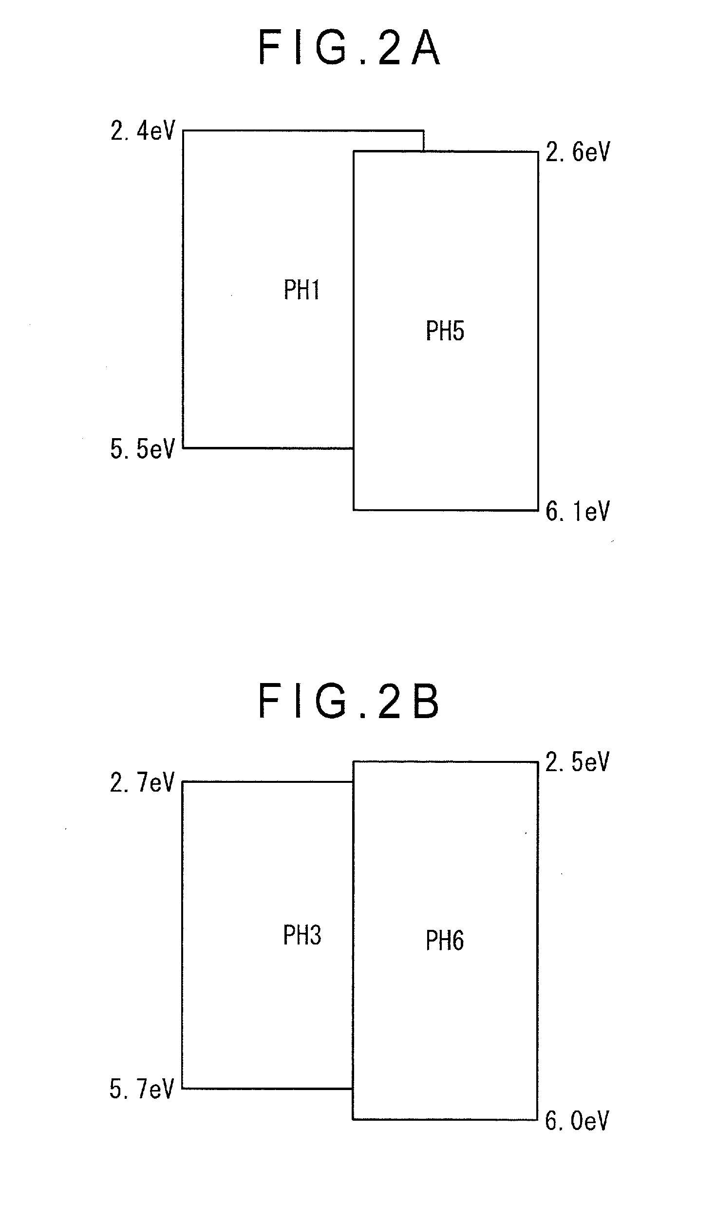
[0240]The organic EL device according to the second exemplary embodiment is different in that the emitting layer includes the first host material, the second host material and the phosphorescent material. In this case, the first host material is the biscarbazole derivative according to the exemplary embodiment represented by the formulae (1) to (3).

[0241]The organic-EL-device material represented by the formulae (1) to (3) has a biscarbazole skeleton having an excellent hole transporting capability and a heterocyclic skeleton having an excellent electron transporting capability, which leads to a bi-polar performance sufficient for functioning as a single host. However, a luminous efficiency and a lifetime of the multilayered organic EL device depend on a carrier balance of an entire organic EL device. Main factors for controlling the carrier balance are carrier transporting capability...

third exemplary embodiment

[0286]An organic EL device according to a third exemplary embodiment is different from the organic EL device according to the second exemplary embodiment in that a material having a poor electron capability is used as the second material.

[0287]When a material having an excellent electron injecting capability from the electrode (e.g., LiF) is used as the cathode, a carrier balance in the emitting layer becomes shifted toward the anode. For improving such a disadvantage, it is preferable to select a material having a poor electron injecting capability as the second host material. Specifically, the second host material of this exemplary embodiment is preferably a compound in which A3 is a group represented by the following formula (7B) in the formula (5) or (6).

(M3)c-(L6)d-(M4)e  (7B)

[0288]In the formula (7B): M3 and M4 each independently represent a substituted or unsubstituted aromatic hydrocarbon group having 6 to 40 ring carbon atoms; M3 and M4 may be the same or different; L6 repr...


PUM

PropertyMeasurementUnit
work functionaaaaaaaaaa
thicknessaaaaaaaaaa
thicknessaaaaaaaaaa

Abstract

A biscarbazole derivative of the invention is represented by a formula (1) below.In the formula (1): A1 represents a substituted or unsubstituted nitrogen-containing heterocyclic group having 1 to 30 ring carbon atoms; A2 represents a substituted or unsubstituted aromatic hydrocarbon group having 6 to 30 ring carbon atoms, or substituted or unsubstituted nitrogen-containing heterocyclic group having 1 to 30 ring carbon atoms; X1 and X2 each are a linking group; Y1 to Y4 each represent a substituent; p and q represent an integer of 1 to 4; and r and s represent an integer of 1 to 3.

Description

CROSS-REFERENCE TO RELATED APPLICATIONS[0001]This application is a Continuation of U.S. Ser. No. 13 / 091,036, filed Apr. 20, 2011, which claims priority from Japanese Patent Application No. 2010-097317, filed Apr. 20, 2010, Japanese Patent Application No. 2010-291138, filed Dec. 27, 2010, U.S. Provisional Application No. 61 / 353,047, filed Jun. 9, 2010, and U.S. Provisional Application No. 61 / 433,084, filed Jan. 14, 2011, the entire contents of which are expressly incorporated by reference herein.BACKGROUND OF THE INVENTION[0002]1. Field of the Invention[0003]The present invention relates to a biscarbazole derivative, a material for an organic electroluminescence device, and an organic electroluminescence device using those.[0004]2. Description of Related Art[0005]A known organic electroluminescence device includes an organic thin-film layer between an anode and a cathode, the organic thin-film layer including an emitting layer, and emits light using exciton energy generated by a reco...

Claims


Application Information

Patent Timeline
Patent Type & Authority Applications(United States)
IPC IPC(8): H01L51/54C07D401/14C07D403/14
CPCC07D209/82C07D403/14C09K11/06C09K2211/1007C09K2211/1029C09K2211/1044C09K2211/1059H05B33/20C09B57/00C07D401/14Y10S428/917H10K85/6572H10K50/11H10K2101/10H10K2101/90H10K50/12H10K85/654H10K50/165H10K50/171
Inventor INOUE, TETSUYAITO, MITSUNORIYOSHIDA, KEIHIBINO, KUMIKONISHIMURA, KAZUKIOGIWARA, TOSHINARIIKEDA, KIYOSHI
Owner IDEMITSU KOSAN CO LTD
Why Eureka
Try Eureka