Interposer and semiconductor device

Active Publication Date: 2012-06-07
NEC CORP
View PDF7 Cites 8 Cited by
  • Summary
  • Abstract
  • Description
  • Claims
  • Application Information

AI Technical Summary

Benefits of technology

[0009]The present invention has been made to solve the issues described above, and provides an interposer that can provide sufficient power supply paths. The interposer makes it possible for a mounting electronic part such as a capacitor or the like to be mounted near the mounting surface of an electronic part (electronic part mounting surface). An object of the present invention is to provide an interposer and a semiconductor device having the interposer which can effectively reduce the power supply noise of the mounted electronic part regardless of the frequency of the noise.
[0014]Thereby, when the mounting electronic part is a capacitor, the high frequency power supply noise generated by the mounted electronic part is effectively reduced by the capacitor, so that a high noise immunity can be achieved.
[0015]In another case, when the mounting electronic part is a resistor part, the transmission characteristics of a series termination circuit can be improved.
[0017]In another case, according to the present invention, as the semiconductor device is provided with the interposer of the present invention, the high frequency power supply noise generated by the mounting electronic part mounted on the interposer can be reduced effectively, and the transmission characteristics of the series termination circuit can be improved. Thereby, the semiconductor device can achieve stable and good operation.

Problems solved by technology

Power supply noise is generated in electronic parts such as a CPU and a clock driver.
However, with this structure, the wiring path where the cavity is formed across the wiring layers is broken.
As a result, the capability of power supply is reduced, and the wiring arrangement of signal lines is degraded.
However, this capacitor sheet has a small capacitance compared to that of general capacitors, so that there is a problem in that the power supply noise cannot be reduced sufficiently.

Method used


Image

  • Interposer and semiconductor device
  • Interposer and semiconductor device
  • Interposer and semiconductor device

Examples


first embodiment

[0032]Next, a description is given of an interposer in accordance with the first embodiment of the present invention.

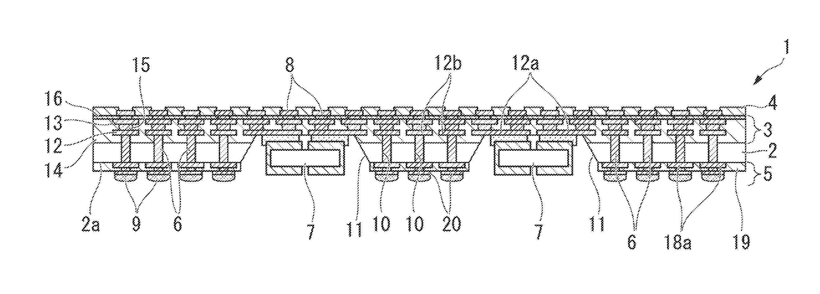
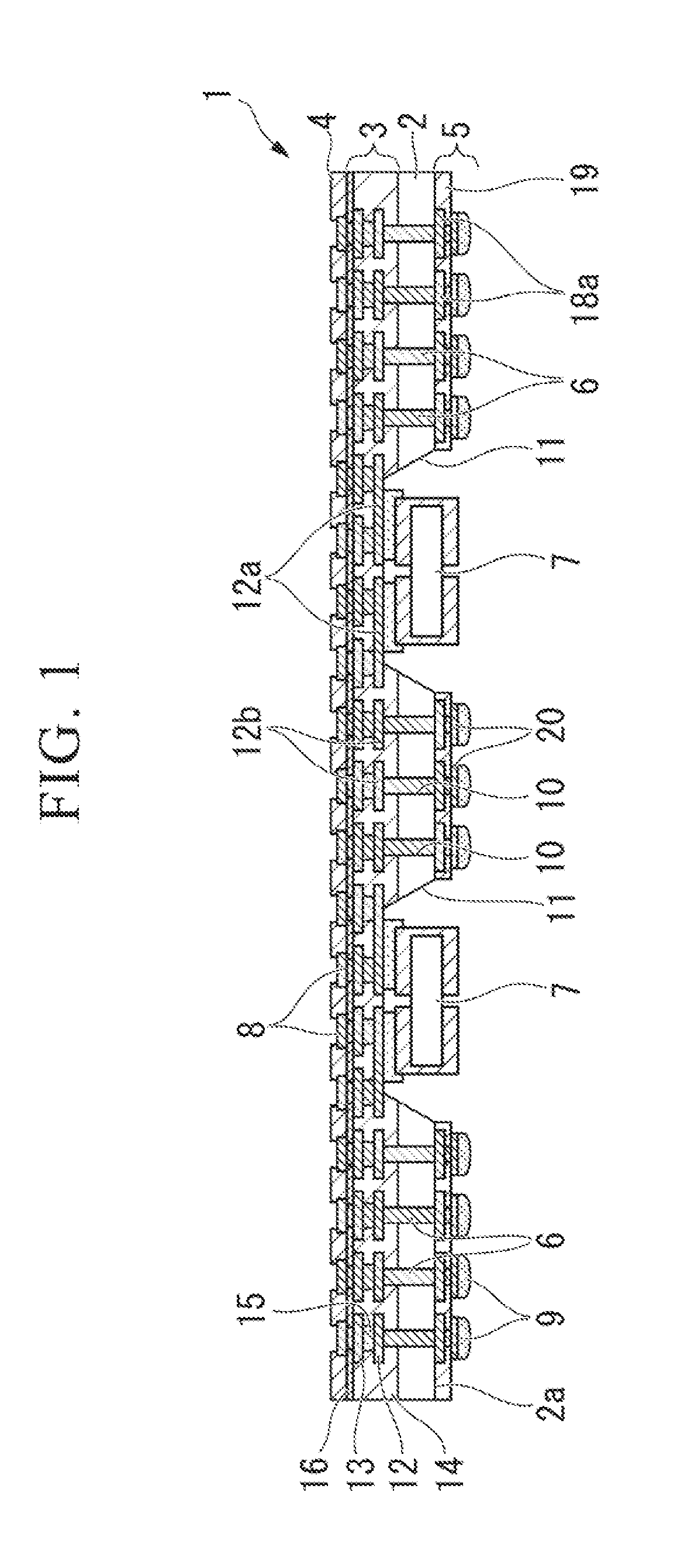
[0033]FIG. 1 is a schematic diagram that illustrates a longitudinal cross-section of an interposer 1 in accordance with a first embodiment of the present invention.

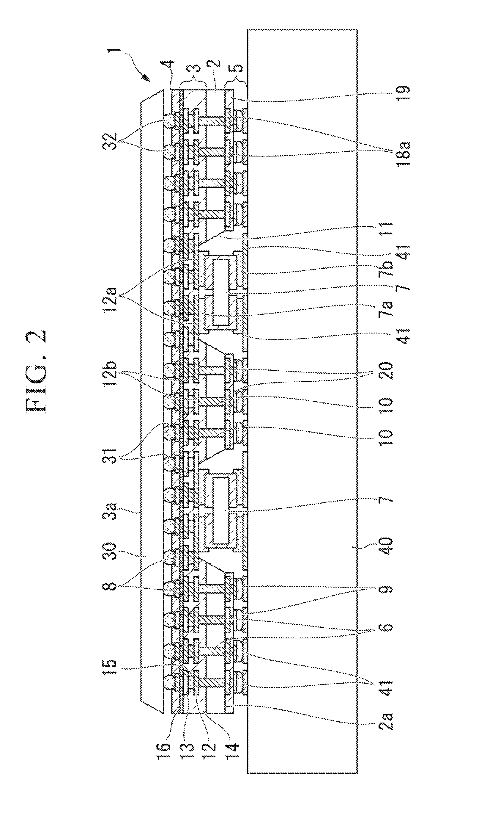
[0034]FIG. 2 is a schematic diagram that illustrates a longitudinal cross-section of the interposer 1, in which an electronic part 30 is mounted on an interposer 1 and the interposer 1 is mounted on a wiring substrate 3.

[0035]The interposer 1 indicated in FIG. 1 includes a silicon substrate 2, a multilayer wiring portion 3, and an encapsulant resin 4 formed on one side surface of the silicon substrate 2, a bump forming portion 5 provided on another side surface of the silicon substrate 2, penetrating electrodes 6 that penetrate the silicon substrate 2 in the thickness direction, and capacitors (electronic parts for mounting) 7 provided in a cavity 11 of the silicon substrate 2. As shown in FIG. 2, with resp...

second embodiment

[0126]Next, a description will be given of an interposer in accordance with the second embodiment.

[0127]In the description of the second embodiment, explanations of the configurations similar to those of the first embodiment are omitted.

[0128]FIG. 8 is a schematic diagram that illustrates a longitudinal cross-section of the interposer in accordance with the second embodiment of the present invention.

[0129]The interposer 1 in accordance with the second embodiment is formed similarly to that of the first embodiment except for the shapes of the penetrating electrodes 6 and the conductive film 18a.

[0130]For the interposer 1, the penetrating electrode 6 is formed by depositing a metal plating film on the inside surface of the penetrating holes 10 with a predetermined thickness, having a ring shape. The conductive film 18a is formed successively from the penetrating electrode 6 at a position close to the end portion of the penetrating electrode 6 of the back surface 2a of the silicon sub...

third embodiment

[0133]Next, a description is given of an interposer 1 in accordance with the third embodiment.

[0134]In the third embodiment, the explanations of the configurations identical to those of the first embodiment are omitted.

[0135]FIG. 9 is a schematic diagram that illustrates a longitudinal cross-section of the interposer 1 in accordance with the third embodiment.

[0136]The interposer 1 in accordance with the third embodiment is configured to have a multiple layer wiring portion 3 that includes six wiring layers consisting of the first wiring layer 12 through the sixth wiring layer 29. The interposer 1 is configured to have the electronic part 30 in which the ground pins are connected to each of the wiring layers 12, 13, 26, 27, 28, and 29 when being mounted on the interposer 1. The configurations of the third embodiment except for the multiple layer wiring portion 3 and the electronic part 30 are similar to those of the first embodiment.

[0137]Based on the third embodiment, the same effec...


PUM


Abstract

An interposer includes a substrate includes a plurality of penetrating electrodes, and a wiring portion formed on the substrate, in which the wiring portion includes a wiring layer electrically connected to the penetrating electrodes and an insulating layer covering the wiring layer. The interposer includes a plurality of first UBM structures provided at a side opposite the substrate of the wiring portion, in which the first UBM structures are electrically connected to the wiring layer. The interposer includes a plurality of bumps provided at the side opposite the wiring portion of the substrate, in which the plurality of bumps is electrically connected to each of the penetrating electrodes via a plurality of second UBM structures.

Description

INCORPORATION BY REFERENCE[0001]Priority is claimed on Japanese Patent Application No. 2010-270079, filed Dec. 3, 2010, the content of which is incorporated herein by reference.BACKGROUND OF THE INVENTION[0002]1. Field of the Invention[0003]The present invention relates to an interposer on which discrete parts such as capacitors are mounted, and to a semiconductor device including the interposer.[0004]2. Description of Related Art[0005]Power supply noise is generated in electronic parts such as a CPU and a clock driver. To reduce the power supply noise, generally, capacitors are employed.[0006]When the frequency of the power noise becomes higher, the capacitors need to be mounted closer to the electronic parts. However, such locations for mounting the capacitors are limited to peripheral rooms of the electronic parts or the back side of an electronic part 104 mounted on an interposer 101 as shown in FIG. 12. Therefore, it is impossible for a capacitor 103 to be placed any closer to ...

Claims


Application Information

Patent Timeline
IPC IPC(8): H01L29/772H01L23/498
CPCH01L23/13H01L23/49811H01L23/49822H01L23/49827H01L2924/15311H01L29/0657H01L2224/16225H01L2224/16227H01L2924/1515H01L23/49833
Inventor TAKEDA, TSUTOMU
Owner NEC CORP
Why Eureka
Try Eureka