PARTIALLY DEPELETED (DP) SEMICONDUCTOR-ON-INSULATOR (SOI) FIELD EFFECT TRANSISTOR (FET) STRUCTURE WITH A GATE-TO-BODY TUNNEL CURRENT REGION FOR THRESHOLD VOLTAGE (Vt) LOWERING AND METHOD OF FORMING THE STRUCTURE

a semiconductor-on-insulator and field-effect transistor technology, applied in the field of dp-dp-dp-dp-dp-dp-dp-dp-dp-dp-dp-dp-dp-dp-dp-dp-dp-dp-dp-dp-dp-dp-dp-dp-dp-dp-dp-dp-dp-dp-dp-

Active Publication Date: 2012-06-14
TAIWAN SEMICON MFG CO LTD
View PDF5 Cites 11 Cited by
  • Summary
  • Abstract
  • Description
  • Claims
  • Application Information

AI Technical Summary

Benefits of technology

[0006]In view of the foregoing, disclosed herein are embodiments of a floating body partially depleted semiconductor-on-insulator field effect transistor (PDSOIFET) structure having a gate-to-body tunnel current region that provides for threshold voltage (Vt) lowering without increasing gate current or other leakage currents. In one embodiment, a semiconductor layer has a center portion with a first conductivity type. A gate structure traverses the center portion. This gate structure has adjacent sections with different conductivity types in order to create, within the center portion of the semiconductor layer, a channel region below one section and a gate-to-body tunnel current region below another section. In another embodiment, a semiconductor layer has a center portion with a channel region and a gate-to-body tunnel current region adjacent to the channel region. The channel region is doped with a dopant having a first conductivity type. The gate-to-body tunnel current region comprises: a first implant region immediately adjacent to the channel region and doped with a higher concentration of the same dopant; a second implant region adjacent to the first implant region and having a second conductivity type; and an enhanced generation and recombination region between the first and second implant regions. A gate structure with the second conductivity type traverses the center portion. The PDSOIFET structure embodiments can, for example, be incorporated into any electronic circuit with some FETs requiring a lower threshold voltage than others (e.g., in an Static Random Access Memory (SRAM) array, where pull-down FETs require a lower threshold voltage that pass-gate or pull-up FETs). Also disclosed herein are embodiments of methods of forming these structures
[0007]More particularly, one embodiment of a field effect transistor, according to the present invention, can comprise a semiconductor layer having end portions and a center portion between the end portions. The center portion can comprise a channel region and a gate-to-body tunnel current region positioned laterally adjacent to the channel region. The channel region and gate-to-body tunnel current region can each have a first conductivity type. A gate structure can traverse the center portion of the semiconductor layer and, specifically, both the channel region and the gate-to-body tunnel current region. This gate structure can comprise a gate dielectric layer on the top surface of the semiconductor layer and a gate conductor layer on the gate dielectric layer. The gate conductor layer can specifically comprise a first conductive section and a second conductive section positioned laterally adjacent to and different from the first conductive section. Specifically, the first conductive section can be positioned on the gate dielectric layer aligned above the gate-to-body tunnel current region and can have the first conductivity type. The second conductive section can be positioned on t

Problems solved by technology

Furthermore, such threshold voltage variations can differ between PDSOIFETs at different locations within an electronic circuit and can, thereby degrade the performan

Method used


Image

  • PARTIALLY DEPELETED (DP) SEMICONDUCTOR-ON-INSULATOR (SOI) FIELD EFFECT TRANSISTOR (FET) STRUCTURE WITH A GATE-TO-BODY TUNNEL CURRENT REGION FOR THRESHOLD VOLTAGE (Vt) LOWERING AND METHOD OF FORMING THE STRUCTURE
  • PARTIALLY DEPELETED (DP) SEMICONDUCTOR-ON-INSULATOR (SOI) FIELD EFFECT TRANSISTOR (FET) STRUCTURE WITH A GATE-TO-BODY TUNNEL CURRENT REGION FOR THRESHOLD VOLTAGE (Vt) LOWERING AND METHOD OF FORMING THE STRUCTURE
  • PARTIALLY DEPELETED (DP) SEMICONDUCTOR-ON-INSULATOR (SOI) FIELD EFFECT TRANSISTOR (FET) STRUCTURE WITH A GATE-TO-BODY TUNNEL CURRENT REGION FOR THRESHOLD VOLTAGE (Vt) LOWERING AND METHOD OF FORMING THE STRUCTURE

Examples


Embodiment Construction

[0033]The embodiments of the invention and the various features and advantageous details thereof are explained more fully with reference to the non-limiting embodiments that are illustrated in the accompanying drawings and detailed in the following description.

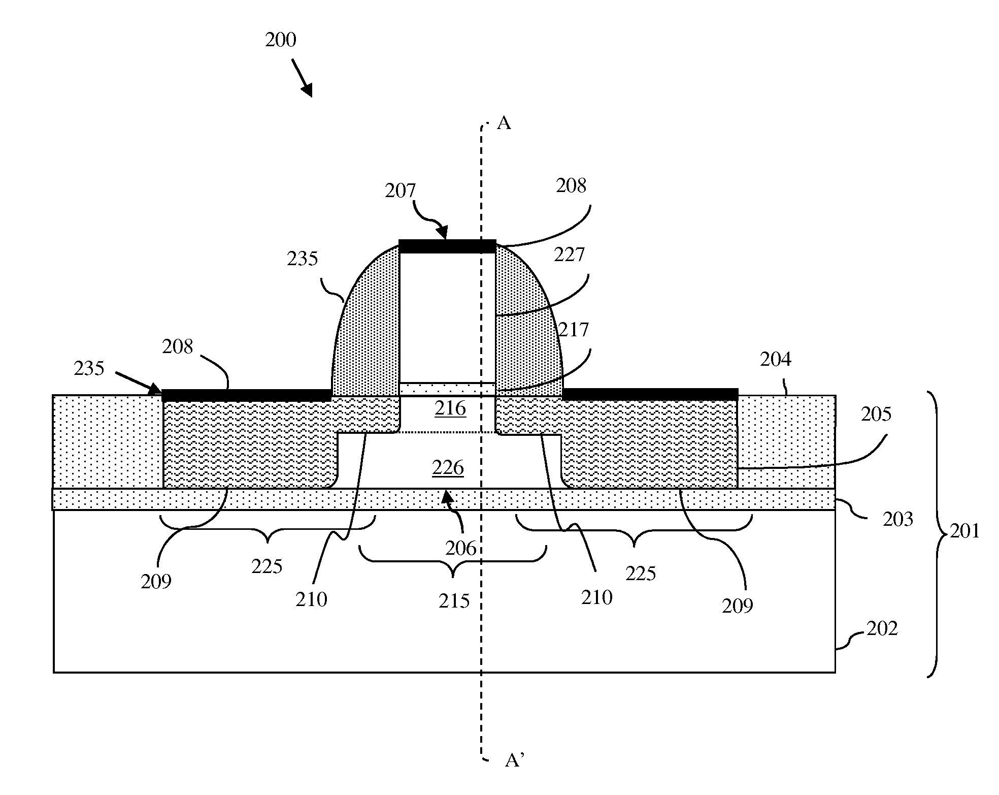
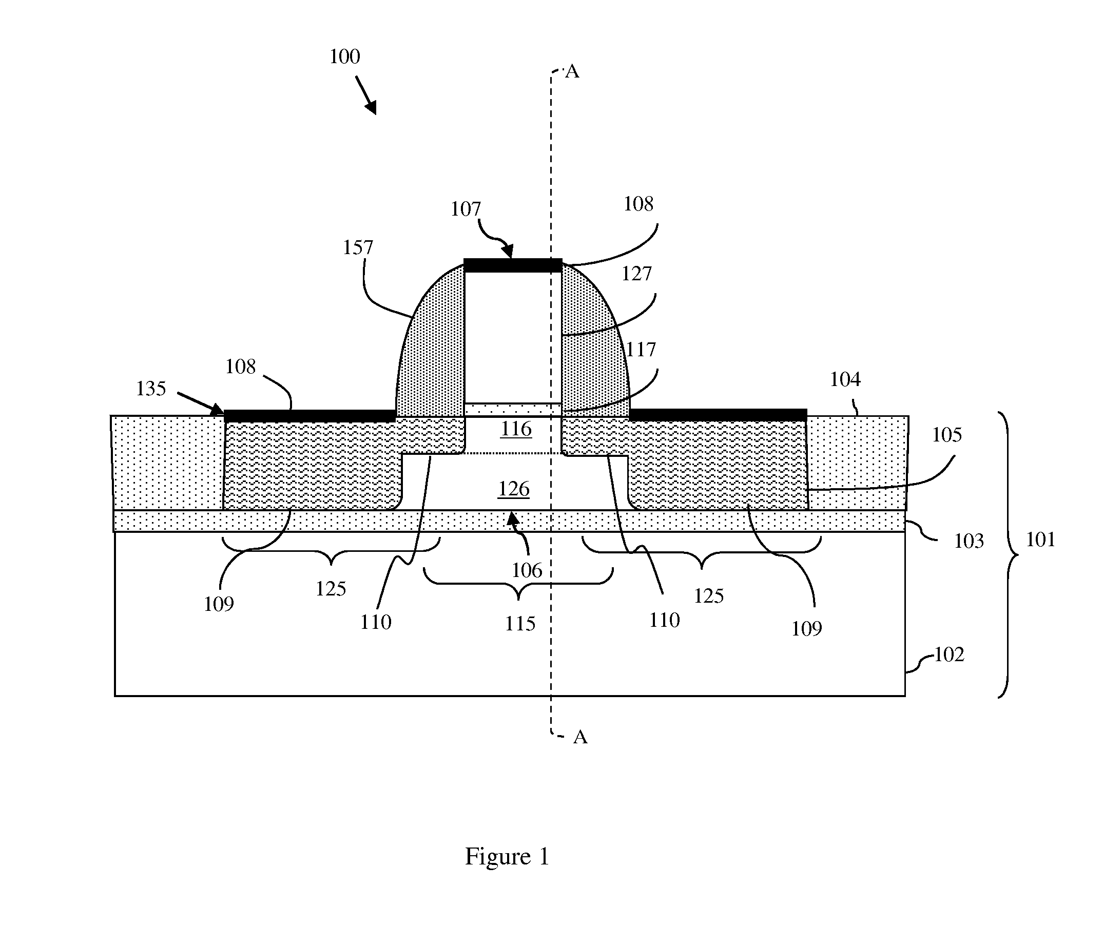
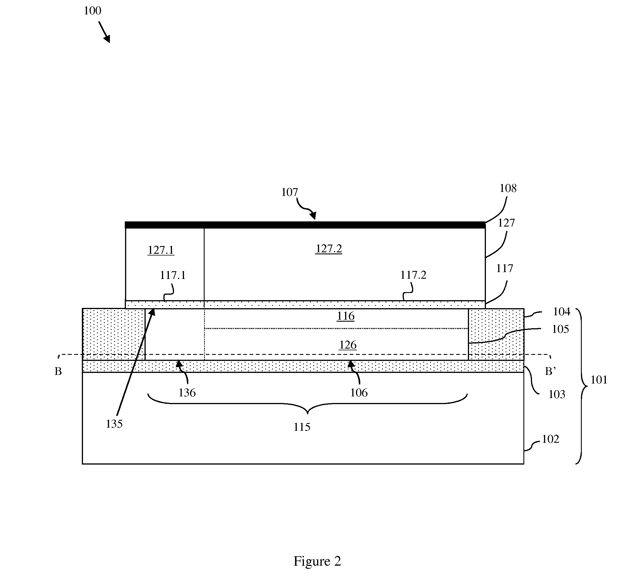
[0034]As mentioned above, a semiconductor-on-insulator (SOI) field effect transistor (FET) is a FET formed in the semiconductor layer of a semiconductor-on-insulator (SOI) wafer. Shallow trench isolations (STI) structures extend through the semiconductor layer and isolate the SOI FET from other devices within the semiconductor layer. As with any FET, an SOIFET comprises a channel region positioned between source / drain regions and a gate structure positioned above the channel region. However, depending upon the configuration of the source / drain regions as well as the thickness of the semiconductor layer, the channel region of the SOIFET may be fully depleted (FD) or partially depleted (PD). Specifically, in a FDSOIFET, the depl...


PUM


Abstract

Disclosed are embodiments of a field effect transistor with a gate-to-body tunnel current region (GTBTCR) and a method. In one embodiment, a gate, having adjacent sections with different conductivity types, traverses the center portion of a semiconductor layer to create, within the center portion, a channel region and a GTBTCR below the adjacent sections having the different conductivity types, respectively. In another embodiment, a semiconductor layer has a center portion with a channel region and a GTBTCR. The GTBTCR comprises: a first implant region adjacent to and doped with a higher concentration of the same first conductivity type dopant as the channel region; a second implant region, having a second conductivity type, adjacent to the first implant region; and an enhanced generation and recombination region between the implant regions. A gate with the second conductivity type traverses the center portion.

Description

BACKGROUND[0001]1. Field of the Invention[0002]The present invention relates to partially depleted (PD) semiconductor-on-insulator (SOI) field effect transistors (FETs) and, more specifically, to embodiments of a PDSOIFET structure with a gate-to-body tunnel current region for threshold voltage (Vt) lowering and a method of forming the PDSOI FET structure.[0003]2. Description of the Related Art[0004]A semiconductor-on-insulator (SOI) field effect transistor (FET) is a FET formed in the semiconductor layer of a semiconductor-on-insulator (SOI) wafer. Shallow trench isolations (STI) structures extend through the semiconductor layer and isolate the SOI FET from other devices within the semiconductor layer. As with any FET, an SOIFET comprises a channel region positioned between source / drain regions and a gate structure positioned above the channel region. However, depending upon the configuration of the source / drain regions as well as the thickness of the semiconductor layer, the chann...

Claims


Application Information

Patent Timeline
IPC IPC(8): H01L29/78H01L21/336
CPCH01L21/26506H01L29/32H01L29/78H01L29/66477H01L29/78612H01L21/26513
Inventor ANDERSON, BRENT A.BRYANT, ANDRESLIANG, JIALENOWAK, EDWARD J.
Owner TAIWAN SEMICON MFG CO LTD
Why Eureka
Try Eureka