Semiconductor element drive device

a technology of magnetic drive and element, applied in the direction of fire alarms, pulse techniques, instruments, etc., can solve the problems of inability to identify anomalous conditions, false detection of alarm signals, complicated configuration of signal formation circuits, etc., to prevent false detection of protection operation conditions, accurately detect integrated time correspondings, and accurate identification of protection circuits

Active Publication Date: 2012-06-14
FUJI ELECTRIC CO LTD
View PDF5 Cites 27 Cited by
  • Summary
  • Abstract
  • Description
  • Claims
  • Application Information

AI Technical Summary

Benefits of technology

[0032]According to the invention, when the semiconductor element drive device which individually drives the semiconductor elements configuring the power converter is provided with the plural protection circuits which detect the information necessary for carrying out a protection operation for the semiconductor elements, pulse signals set to have pulse widths differing from one of the plural protection circuits to another are prevented from being output at the same time. For this reason, it is possible to obtain an advantage in that it is possible to accurately identify a protection circuit with the pulse width of a pulse signal, and that it is possible to prevent a false detection of a protection operation condition.
[0033]Also, one pulse corresponding to the pulse width of an anomalous pulse signal among continuous pulse signals output from the pulse signal output circuit is output as the notification signal by the notification signal output circuit, meaning that there is no need to detect a total time of plural pulses, and it is possible to accurately detect an integrated time corresponding to the pulse width.
[0034]Furthermore, one pulse's worth of notification signal corresponding to the pulse width of an anomalous pulse signal among continuous pulse signals output from the pulse signal output circuit is output by the notification signal output circuit, plural times, maintaining predetermined intervals, meaning that it is possible to reliably carry out a protection operation notification to the exterior without falsely determining that there is an operation notification signal.

Problems solved by technology

For this reason, there is an unsolved problem in that, when an alarm signal is output from another alarm unit before the alarm signals are returned simultaneously, or one alarm signal is returned, to an on condition by the plural alarm units, the alarm signal is falsely detected.
Also, in the heretofore known example described in JP-A-2002-27665, there is an unsolved problem in that it is necessary to output two kinds of signal, an alarm signal and an anomaly factor identification signal, resulting in a complicated configuration of a signal formation circuit.
However, in the heretofore known example described in JP-A-2000-341960, there is an unsolved problem in that, it not being possible to identify the collector current or chip temperature, it is only possible to determine whether there is a condition in which an anomaly has occurred or there is a sign of the anomaly occurrence before that, and it is not possible to identify an anomalous condition.
Also, in the heretofore known example described in JP-A-2007-324828, a configuration is such that, in order to prevent the inverter being stopped by a false signal from the protection circuit, the command unit determines that there is an anomaly when the number of counts, wherein the number of anomaly notifications received from the protection circuit is counted, is two or more, but there is an unsolved problem in that it is not possible to simply identify an anomalous condition.
However, as well as it being difficult to accurately determine the kind of the anomaly with the size of the duty, the PWM pulse is output while the anomaly is continuing, meaning that when the duty ratio becomes higher, the interval between adjacent pulses becomes narrower.
For this reason, in the heretofore known example described in JP-A-2007-82360, as a total time of the repeatedly output PWM pulses is measured, there is an unsolved problem in that an error is liable to occur in the measurement of the alarm time, and it is difficult to accurately determine the kind of an anomaly.

Method used


Image

  • Semiconductor element drive device
  • Semiconductor element drive device
  • Semiconductor element drive device

Examples


second embodiment

[0087]Next, a description will be given of a second embodiment, referring to FIG. 6.

[0088]In the second embodiment, as in the first embodiment, a configuration is such as to switch the protection operation notification signal Sn to the low level plural times in accordance with the pulse train signals PSvd, PSoc, and PSoh which are the alarm signals, and make plural protection operation notifications to the external control device.

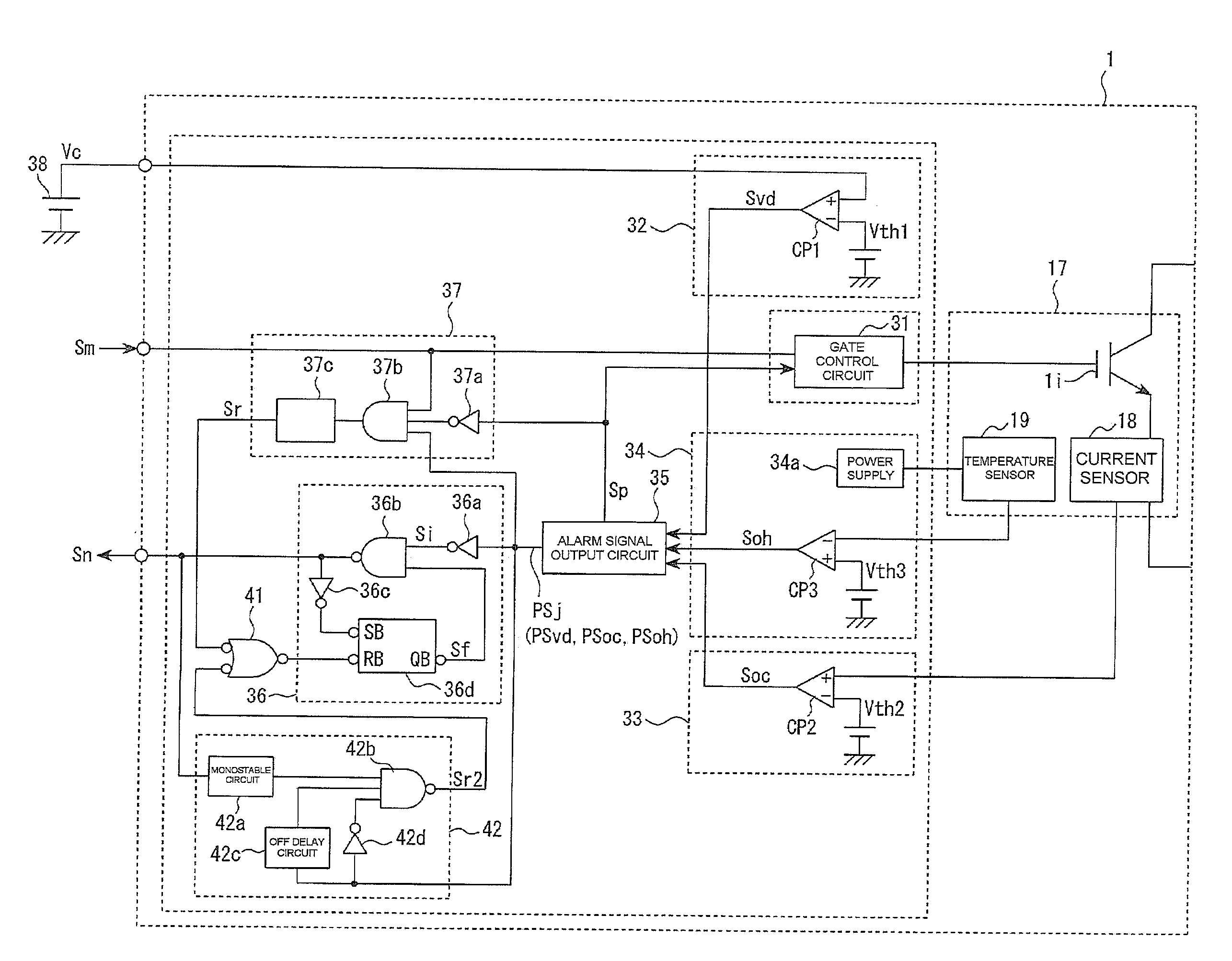
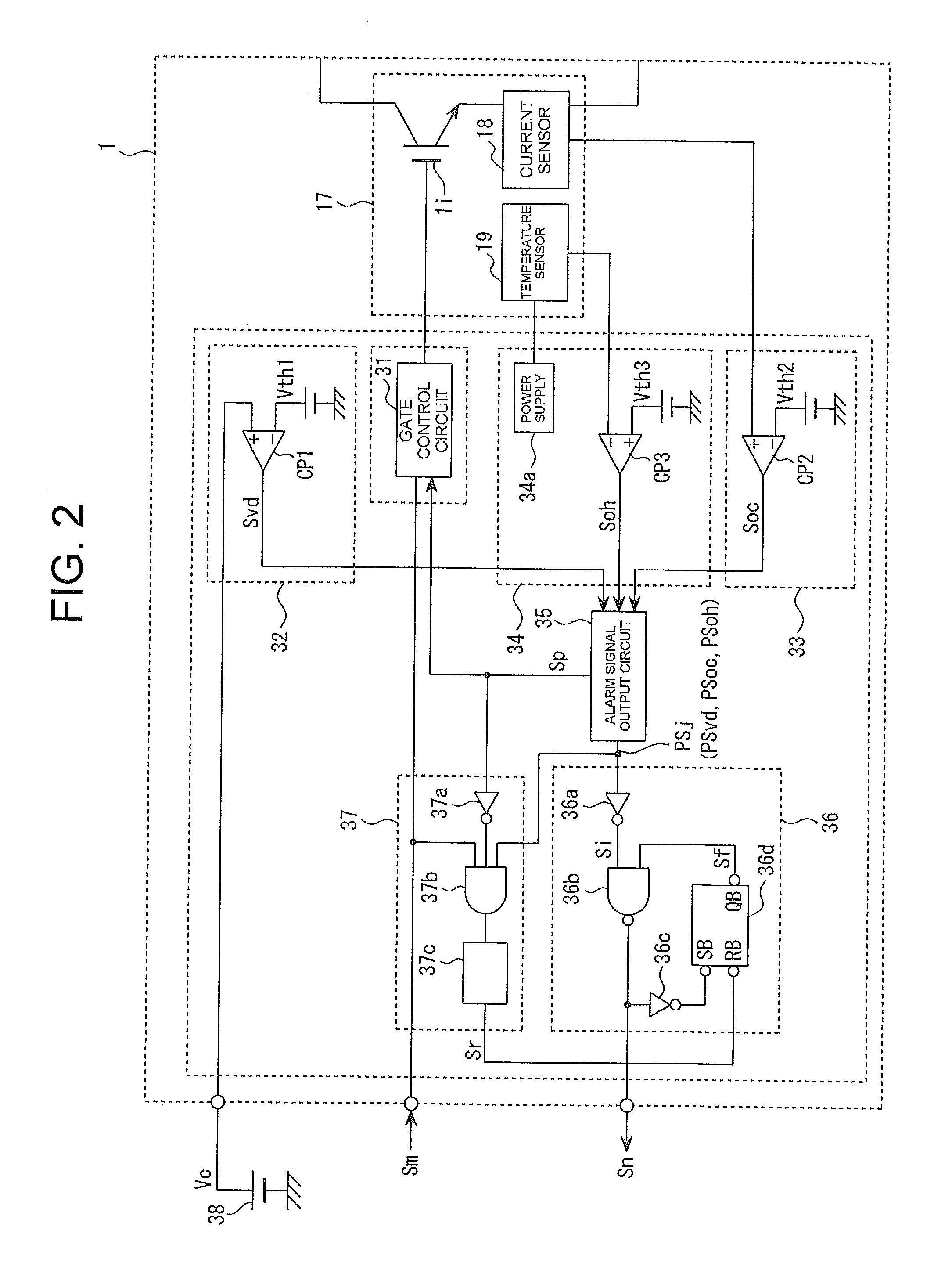
[0089]That is, in the second embodiment, as shown in FIG. 6, in the heretofore described configuration of FIG. 2 of the first embodiment, a NOR gate 41 having inverting input terminals is inserted between the reset signal formation circuit 37 and the inverting reset terminal RB of the RS type flip-flop circuit 36d. The reset signal Sr output from the reset signal formation circuit 37 is input into one inverting input side of the NOR gate 41, and a second reset signal Sr2 output from a protection operation notification continuation circuit 42 is input into t...

first embodiment

[0096]In this normal condition, in the same way as in the first embodiment, at a point t10, the low voltage detection signal Svd output from the control voltage detection circuit 32 of each driver circuit 3U to 3Z, the overcurrent detection signal Soc output from the overcurrent detection circuit 33, and the overheat detection signal Soh output from the chip temperature detection circuit 34 are all at the low level, as shown in FIG. 7B, and as well as the alarm signal output from the alarm signal output circuit 35 maintaining the high level, the protection signal Sp also maintains the low level, as shown in FIG. 7E.

[0097]At this time, the reset signal Sr output from the reset pulse formation circuit 37 maintains the low level, as shown in FIG. 7C.

[0098]At this time, with the notification signal output circuit 36, the alarm signal PSj output from the alarm signal output circuit 35 maintains the high level, as shown in FIG. 7D, and the inverting pulse train signal Si output from the l...


PUM


Abstract

A semiconductor element drive device which individually drives semiconductor elements configuring a power converter includes plural protection circuits which detect information necessary for carrying out a protection operation for the semiconductor elements, an alarm signal output circuit which, having set therein pulse signals with pulse widths differing from one of the plural protection circuits to another, continuously outputs a pulse signal corresponding to a protection circuit, among the plural protection circuits, which has first detected that a protection operation is necessary, as an alarm signal during a period in which it is detected that the protection operation is necessary, and a notification signal output circuit which, when the alarm signal is output from the alarm signal output circuit, outputs one pulse thereof equivalent to the set pulse width as a protection operation notification signal.

Description

CROSS-REFERENCE TO RELATED APPLICATIONS[0001]This application claims priority under 35 U.S.C. §119 from Japanese Patent Application No. 2010-277689, filed on Dec. 14, 2010, and from Japanese Patent Application No. 2001-168512, filed on Aug. 1, 2011. The entirety of each of the identified applications is incorporated herein by reference.BACKGROUND OF THE INVENTION[0002]1. Technical Field[0003]The present invention relates to a semiconductor element drive device which, as well as driving a semiconductor element configuring, for example, a power converter, has a function of identifying a protection operation.[0004]2. Related Art[0005]As this kind of semiconductor element drive device, for example, an alarm circuit described in JP-A-08-70580 is known. In this heretofore known example described in JP-A-08-70580, an intelligent power module (IPM), which is a power transistor module driving an inverter, includes an overcurrent alarm unit, an overvoltage alarm unit, and an overheat alarm un...

Claims


Application Information

Patent Timeline
Patent Type & Authority Applications(United States)
IPC IPC(8): G08B23/00G08B17/00G08B21/00
CPCH03K17/0822H03K17/18H03K2017/0806
Inventor KOMATSU, SACHIAKIMOTOHASHI, SATORU
Owner FUJI ELECTRIC CO LTD
Why Eureka
Try Eureka