Scanning signal line drive circuit and display device including same

a drive circuit and signal line technology, applied in semiconductor devices, instruments, computing, etc., can solve the problem that each source bus line cannot transmit video signals indicating pixel values for a plurality of rows, and achieve the effect of facilitating shift register testing, improving panel yield, and relatively easy repair

Inactive Publication Date: 2012-06-14
SHARP KK
View PDF2 Cites 20 Cited by
  • Summary
  • Abstract
  • Description
  • Claims
  • Application Information

AI Technical Summary

Benefits of technology

[0042]According to the first aspect of the present invention, the shift register is grouped every k consecutive stages, and different types of marks are respectively formed on circuits of k stages included in each group such that the same type of mark appears every k stages. Hence, a plurality of stages forming the shift register can be distinguished from one another. By this, shift register testing is facilitated over conventional cases and thus even if a failure occurs in the shift register at a panel fabrication stage, the failure is repaired relatively easily, improving panel yields.
[0043]According to the second aspect of the present invention, the shift resister is grouped every some stages, the number of which is equal to the number of clock signals. For (a plurality of) stages to which a plurality of clock signals are provided in the same manner, the same type of marks are formed. Hence, when some kind of failure occurs in the shift register at a panel fabrication stage, it can be easily grasped, based on a mark, how clock signals are provided to a circuit of a stage where the failure has occurred. By this, shift register testing is greatly facilitated over conventional cases and thus even if a failure occurs in the shift register at a panel fabrication stage,

Problems solved by technology

However, each source bus line cannot transmit video signals indicat

Method used


Image

  • Scanning signal line drive circuit and display device including same
  • Scanning signal line drive circuit and display device including same
  • Scanning signal line drive circuit and display device including same

Examples


Embodiment Construction

[0076]An embodiment of the present invention will be described below with reference to the accompanying drawings.

[0077]

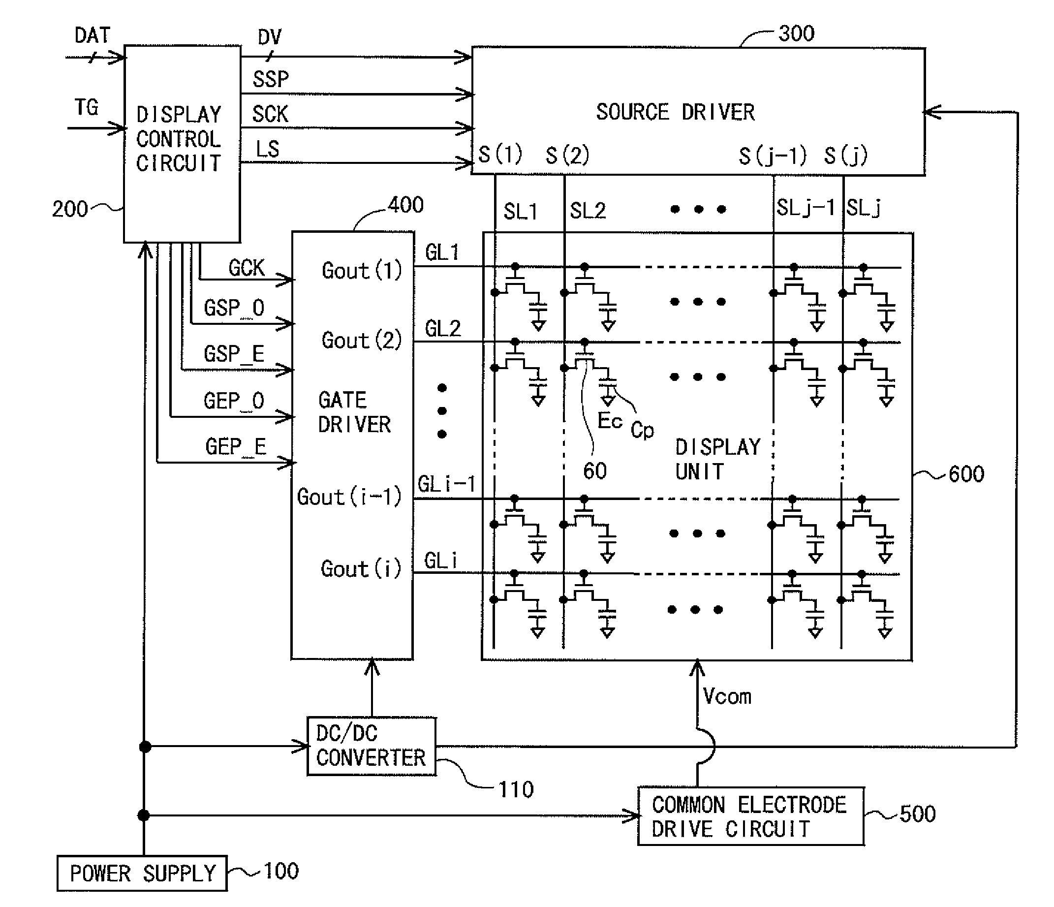
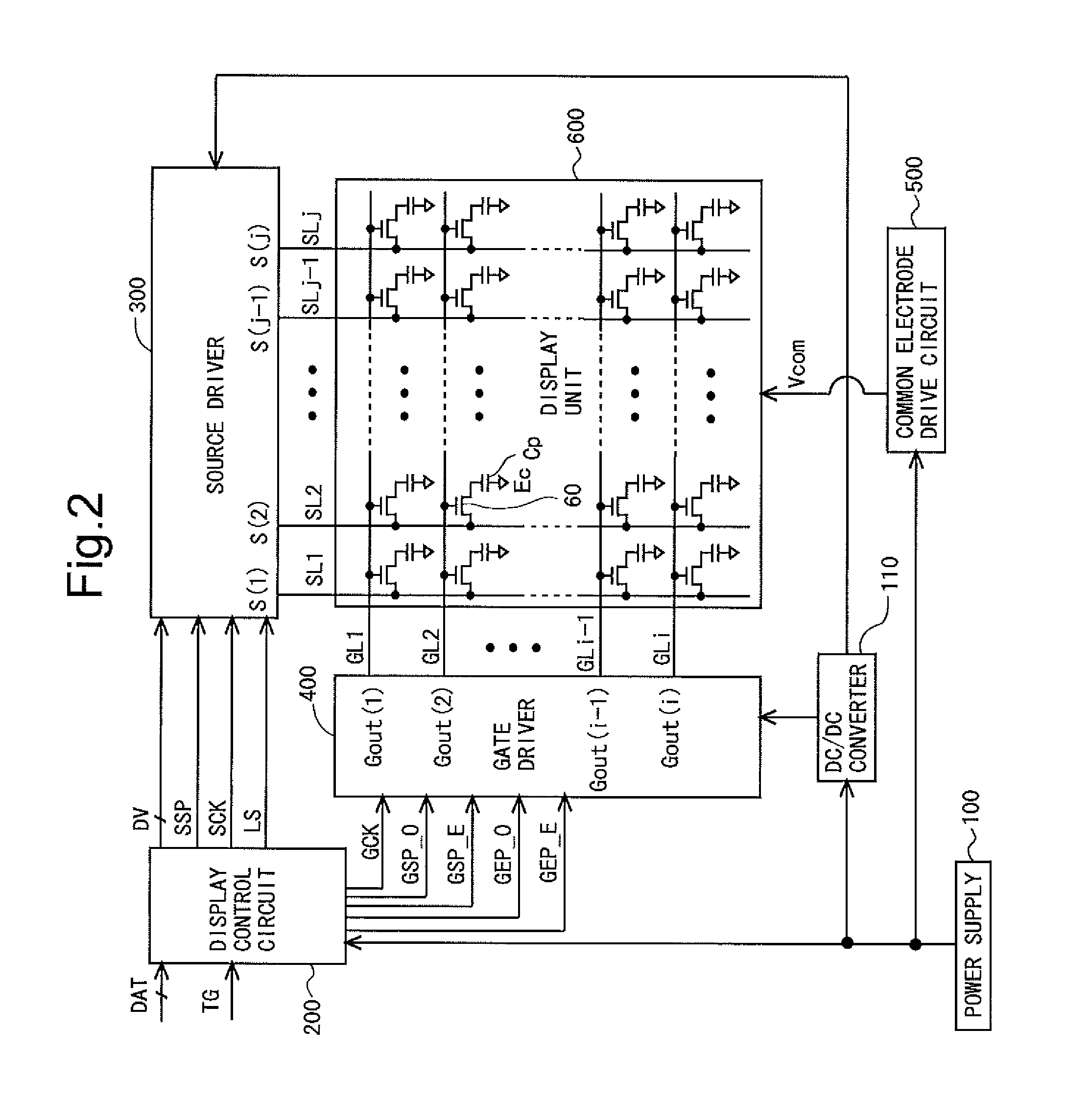
[0078]FIG. 2 is a block diagram showing an overall configuration of an active matrix-type liquid crystal display device according to an embodiment of the present invention. As shown in FIG. 2, the liquid crystal display device includes a power supply 100, a DC / DC converter 110, a display control circuit 200, a source driver (video signal line drive circuit) 300, a gate driver (scanning signal line drive circuit) 400, a common electrode drive circuit 500, and a display unit 600. Note that in the present embodiment the gate driver 400 and the display unit 600 are formed on the same substrate. Namely, the gate driver 400 in the present embodiment is a “monolithic gate driver”.

[0079]The display unit 600 includes a plurality of (j) source bus lines (video signal lines) SL1 to SLj; a plurality of (i) gate bus lines (scanning signal lines) GL1 to GLi; and a plurality of (i...


PUM


Abstract

A gate driver is implemented that includes an easily testable shift register to improve panel yields. In a monolithic gate driver including a shift register that operates based on 4-phase clock signals, each stage of the shift register is provided with an inter-stage connecting wiring line for receiving a clock signal other than clock signals received from a clock signal trunk wiring line, from a different stage than the stage; and a contact that connects a wiring line formed on the stage to the inter-stage connecting wiring line. The shift register is grouped every four consecutive stages. Markings formed of different numbers of planar-view circular-shaped structures are formed on bistable circuits of four stages included in each group such that the same type of marking appears every four stages.

Description

TECHNICAL FIELD[0001]The present invention relates to a scanning signal line drive circuit of an active matrix-type display device, and more specifically to a layout of a shift register provided in a scanning signal line drive circuit.BACKGROUND ART[0002]Conventionally, there is known an active matrix-type display device in which a plurality of gate bus lines (scanning signal lines) and a plurality of source bus lines (video signal lines) are arranged in a grid pattern and a plurality of pixel formation portions are arranged in a matrix form at the respective intersections of the plurality of gate bus lines and the plurality of source bus lines. Each pixel formation portion includes a TFT (Thin Film Transistor) which is a switching element connected at its gate terminal to a gate bus line passing through a corresponding intersection, and connected at its source terminal to a source bus line passing through the intersection; a pixel capacitance for holding a pixel value; and the like...

Claims


Application Information

Patent Timeline
IPC IPC(8): G09G5/00
CPCG02F1/13454H01L27/124G09G2310/0286G09G3/3266
Inventor SAKAMOTO, MAYUKOYONEMARU, MASASHIISHII, KENICHINAKAMIZO, MASAHIKO
Owner SHARP KK
Why Eureka
Try Eureka