METHOD OF FORMING TITANIUM NITRADE (TiN) FILM, NONVOLATILE MEMORY DEVICE USING THE TiN FILM, AND METHOD OF MANUFACTURING THE NONVOLATILE MEMORY DEVICE

a technology of titanium nitrade and nonvolatile memory, which is applied in the direction of solid-state devices, coatings, chemical vapor deposition coatings, etc., can solve the problems of degrading the reliability characteristics of the device, reducing the number of write pulses used in the write operation, and reducing the reliability of the device. , to achieve the effect of increasing the durability characteristics

Inactive Publication Date: 2012-06-14
SAMSUNG ELECTRONICS CO LTD
View PDF3 Cites 18 Cited by
  • Summary
  • Abstract
  • Description
  • Claims
  • Application Information

AI Technical Summary

Benefits of technology

[0009]Exemplary embodiments of the present invention provide a method of manufacturing a nonvolatile memory device with increased durability characteristics.
[0010]Exemplary embodiments of the present invention also provide a method of forming a TiN film which constitutes a nonvolatile memory device with improved durability characteristics.
[0011]Exemplary embodiments of the present invention also provide a nonvolatile memory device with increased durability characteristics.

Problems solved by technology

A significant issue in increasing the integration density of such a PRAM is a reduction in the number of write pulses used in a write operation.
However, these methods may be difficult to apply in an actual process.
Even when the methods are applied, various defects may occur, thereby degrading the reliability characteristics of a device.

Method used


Image

  • METHOD OF FORMING TITANIUM NITRADE (TiN) FILM, NONVOLATILE MEMORY DEVICE USING THE TiN FILM, AND METHOD OF MANUFACTURING THE NONVOLATILE MEMORY DEVICE
  • METHOD OF FORMING TITANIUM NITRADE (TiN) FILM, NONVOLATILE MEMORY DEVICE USING THE TiN FILM, AND METHOD OF MANUFACTURING THE NONVOLATILE MEMORY DEVICE
  • METHOD OF FORMING TITANIUM NITRADE (TiN) FILM, NONVOLATILE MEMORY DEVICE USING THE TiN FILM, AND METHOD OF MANUFACTURING THE NONVOLATILE MEMORY DEVICE

Examples


Embodiment Construction

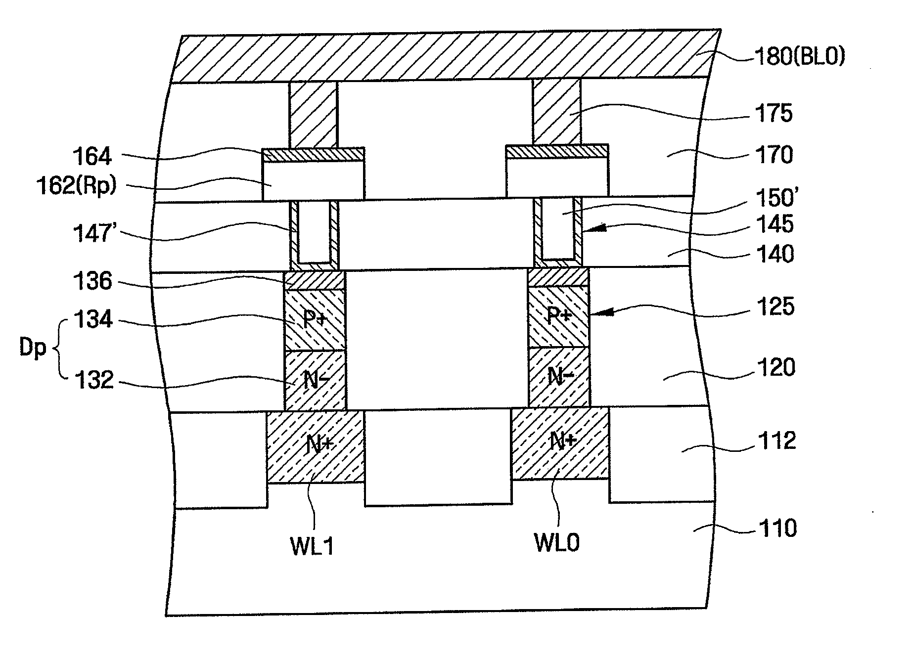
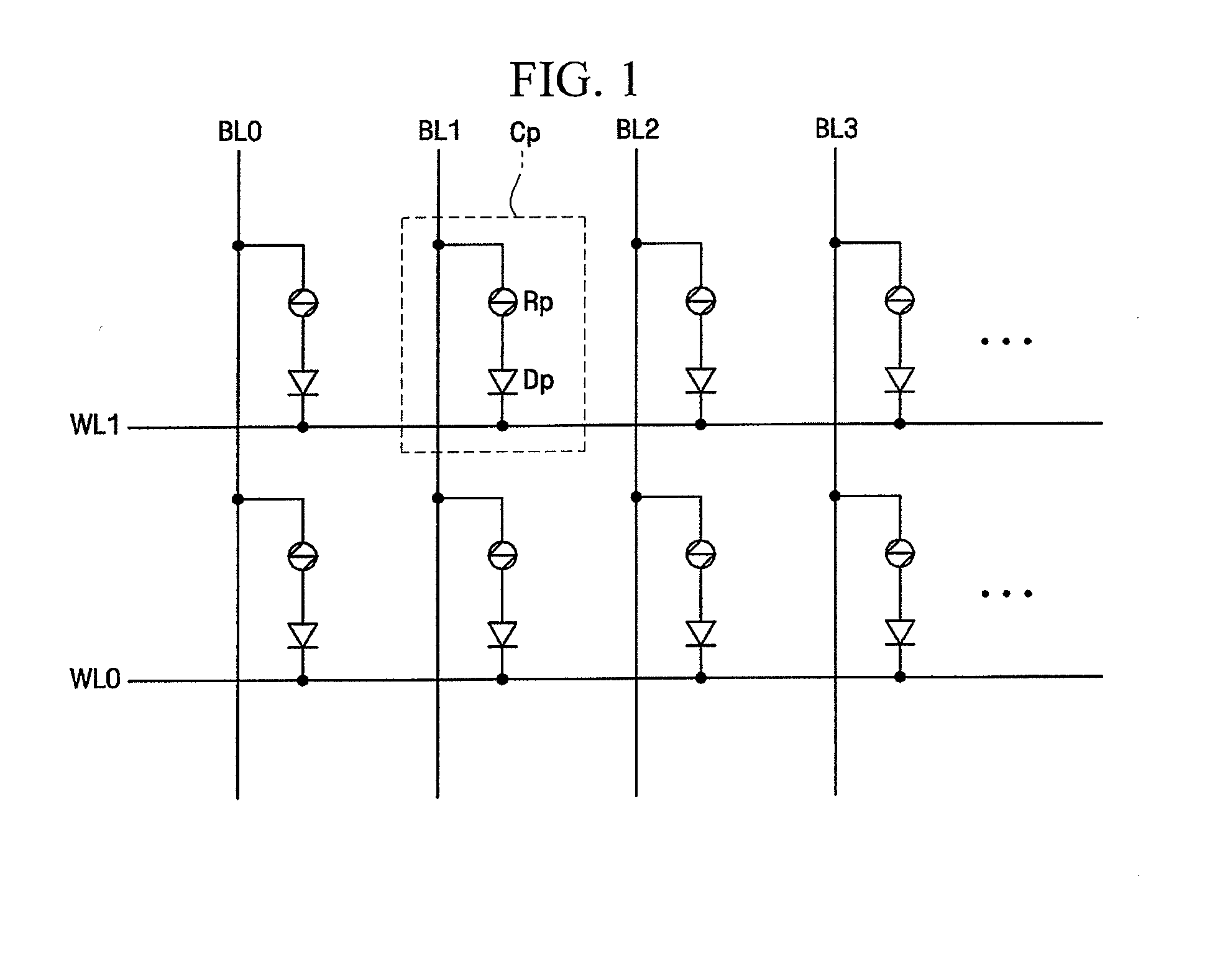
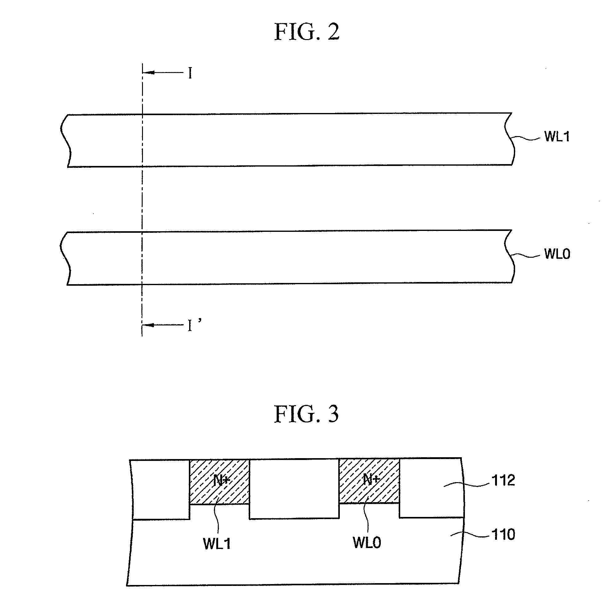
[0020]Exemplary embodiments of the present invention will now be described more fully hereinafter with reference to the accompanying drawings, in which exemplary embodiments of the invention are shown. Exemplary embodiments of the present invention may, however, be embodied in different forms and should not be construed as limited to exemplary embodiments set forth herein. The same reference numbers indicate the same components throughout the specification.

[0021]It will be understood that when an element or layer is referred to as being “connected to,” or “coupled to” another element or layer, it can be directly connected to or coupled to another element or layer or intervening elements or layers may be present. Like numbers refer to like elements throughout. As used herein, the term “and / or” includes any and all combinations of one or more of the associated listed items.

[0022]Hereinafter, exemplary embodiments of the present invention will be described using a phase-change random a...


PUM

PropertyMeasurementUnit
temperatureaaaaaaaaaa
write currentaaaaaaaaaa

Abstract

A method of manufacturing a nonvolatile memory device includes forming an insulating film pattern, which includes apertures, on a substrate, forming a switching element in each of the apertures, forming a bottom electrode on the switching element by using a silicon (Si)-doped titanium nitride (TiN) film, and forming a variable resistance material pattern on the bottom electrode. The Si-doped TiN film is formed by repeatedly forming a TiN film and doping the TiN film with Si.

Description

[0001]This application claims priority from Korean Patent Application No. 10-2010-0127107 filed on Dec. 13, 2010, the disclosure of which is hereby incorporated by reference herein in its entirety.BACKGROUND[0002]1. Technical Field[0003]Exemplary embodiments of the present invention relate to a nonvolatile memory device and a method of manufacturing the same.[0004]2. Description of the Related Art[0005]Examples of nonvolatile memories using resistance materials include phase-change random access memories (PRAMs), resistive RAMs (RRAMs), and magnetic RAMs (MRAMs). While dynamic RAMs (DRAMs) or flash memories store may data using charges, nonvolatile memories using resistance materials may store data using a state change of a phase-change material such as, for example, chalcogenide alloy (in the case of PRAMs), a resistance change of a variable resistance material (in the case of RRAMs), or a resistance change of a magnetic tunnel junction (MTJ) thin film according to a magnetization ...

Claims


Application Information

Patent Timeline
Patent Type & Authority Applications(United States)
IPC IPC(8): H01L21/20H01L21/768
CPCC23C16/34C23C16/45529H01L27/2409H01L27/2463H01L45/141H01L45/16H01L45/1233H01L45/126H01L45/143H01L45/144H01L45/06H10B63/20H10B63/80H10N70/8413H10N70/8825H10N70/882H10N70/231H10N70/011H10N70/8828H10N70/826H10N70/061
Inventor PARK, YOUNG-LIMLEE, JIN-ILCHUNG, KYUNG-MINJUNG, SUG-WOOKIM, CHANG-SU
Owner SAMSUNG ELECTRONICS CO LTD
Why Eureka
Try Eureka