Method of controlling semiconductor process distribution

a technology of semiconductor process and control method, applied in the field of semiconductor process, can solve problems such as poor or inconsistent process distribution

Active Publication Date: 2012-06-14
SAMSUNG ELECTRONICS CO LTD
View PDF10 Cites 12 Cited by
  • Summary
  • Abstract
  • Description
  • Claims
  • Application Information

AI Technical Summary

Benefits of technology

[0007]Exemplary embodiments of the inventive concept provide a method of controlling semiconductor process distribution that is us

Problems solved by technology

When the process capability of the semiconductor wafer processing apparatus changes, poor or inconsistent process distribution may occur.
As process distribution changes, th

Method used


Image

  • Method of controlling semiconductor process distribution
  • Method of controlling semiconductor process distribution
  • Method of controlling semiconductor process distribution

Examples


Embodiment Construction

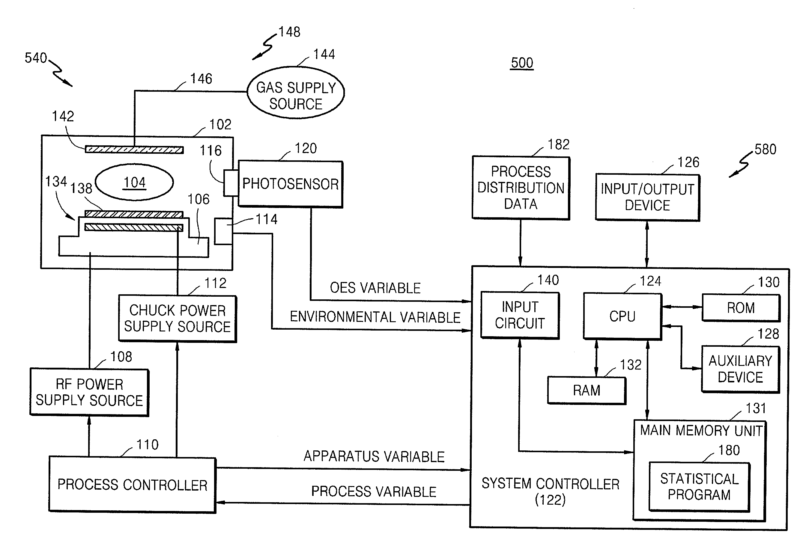
[0042]Exemplary embodiments of the inventive concept will be described more fully hereinafter with reference to the accompanying drawings. Like reference numerals may refer to like elements throughout the accompanying drawings.

[0043]As will be appreciated by one skilled in the art, aspects of the inventive concept may be embodied as a system, method, computer program product, or a computer program product embodied in one or more computer readable medium(s) having computer readable program code embodied thereon. The computer readable program code may be provided to a processor of a general purpose computer, special purpose computer, or other programmable data processing apparatus. The computer readable medium may be a computer readable signal medium or a computer readable storage medium. The computer readable storage medium may be any tangible medium that can contain, or store a program for use by or in connection with an instruction execution system, apparatus, or device.

[0044]In a ...


PUM


Abstract

A method of controlling process distribution of a semiconductor process includes receiving process distribution data representing the process distribution of the semiconductor process, receiving a parameter related to the process distribution, generating a virtual metrology model corresponding to the process distribution based on a relationship between the process distribution data and the parameter, and modifying a process variable affecting the process distribution based on the virtual metrology model.

Description

CROSS-REFERENCE TO RELATED APPLICATIONS[0001]This application claims priority under 35 U.S.C. §119 to Korean Patent Application No. 10-2010-0125656, filed on Dec. 9, 2010, the disclosure of which is incorporated by reference herein in its entirety.BACKGROUND[0002]1. Technical Field[0003]Exemplary embodiments of the inventive concept relate to a semiconductor process, and more particularly, to a method of controlling semiconductor process distribution.[0004]2. Discussion of the Related Art[0005]A semiconductor process may be classified as a deposition process, an ion implantation process, a photolithography process, or an etching process. A semiconductor device is manufactured by performing the above-described semiconductor processes on a single semiconductor wafer multiple times.[0006]The process capability of a semiconductor wafer processing apparatus may vary due to various factors. When the process capability of the semiconductor wafer processing apparatus changes, poor or incons...

Claims


Application Information

Patent Timeline
IPC IPC(8): G05B13/04
CPCG05B19/41875G05B2219/32191G05B2219/35346H01L21/67253G05B21/00G05B2219/32187G05B2219/45031Y02P90/02Y02P90/80
Inventor LEE, HO-KIBAEK, KYE-HYUNLEE, YOUNG-CHUELMIN, GYUNG-JIN
Owner SAMSUNG ELECTRONICS CO LTD
Why Eureka
Try Eureka