
Process for treating a semiconductor wafer

a technology for cleaning surfaces and semiconductor wafers, applied in cleaning processes and equipment, detergent compositions, electrical equipment, etc., can solve the problems of increased cost of ownership, prolonged rinsing period, and lower throughput, and achieve the effect of quick and effective removal of the surface of the wafer

Inactive Publication Date: 2012-06-28
LAM RES AG
View PDF3 Cites 1 Cited by
  • Summary
  • Abstract
  • Description
  • Claims
  • Application Information

AI Technical Summary

Benefits of technology

[0009]The present inventors have discovered that highly concentrated inorganic acids used in a stripping operation during the processing of semiconductor wafers can be more quickly and effectively removed from the wafer surface by rinsing with a liquid that is itself a relatively concentrated solution of strong inorganic acid and contains a controlled quantity of fluoride ion.

Problems solved by technology

However, highly concentrated inorganic acids, and especially sulfuric acid, are highly viscous, and it therefore requires an extended period of rinsing to remove the acid-based cleaning liquid from the wafer surface.
In addition, when using an SC-1 mixture significant equipment problems arise due to crystal formation in the exhaust and drain lines, those crystals being the product of ammonia vapor reacting with sulfate residues to form for example ammonium sulfate and ammonium bisulfate.
This protracted removal step also leads to higher cost of ownership and lower throughput due to higher chemical consumption and long process times.
Similarly, semiconductor processing already consumes substantial volumes of deionized ultrapure water (UPW), which can have a negative environmental impact, especially given that the current generation of 300 mm wafer has more than twice the surface area of the previous 200 mm wafer.

Method used


Image

  • Process for treating a semiconductor wafer
  • Process for treating a semiconductor wafer
  • Process for treating a semiconductor wafer

Examples


Embodiment Construction

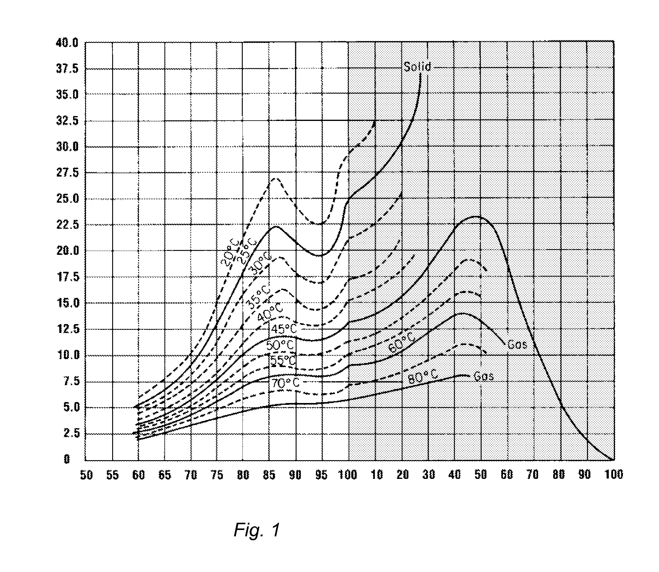
[0017]Concentrated solutions of inorganic acids are generally of high viscosity. In FIG. 1, the properties of sulfuric acid are shown, with the units of the ordinate being viscosity in cP and those of the abscissa being % concentration. The left side of the figure shows increasing concentrations of aqueous solutions of sulfuric acid, whereas the right side shows increasing concentrations of oleum, i.e., compositions in which the sulfuric acid has reached 100% and sulfur trioxide is present in increasing concentration.

[0018]In general the viscosity of such solutions increases markedly with increasing strength of inorganic acid, with the effect being more pronounced at lower temperatures.

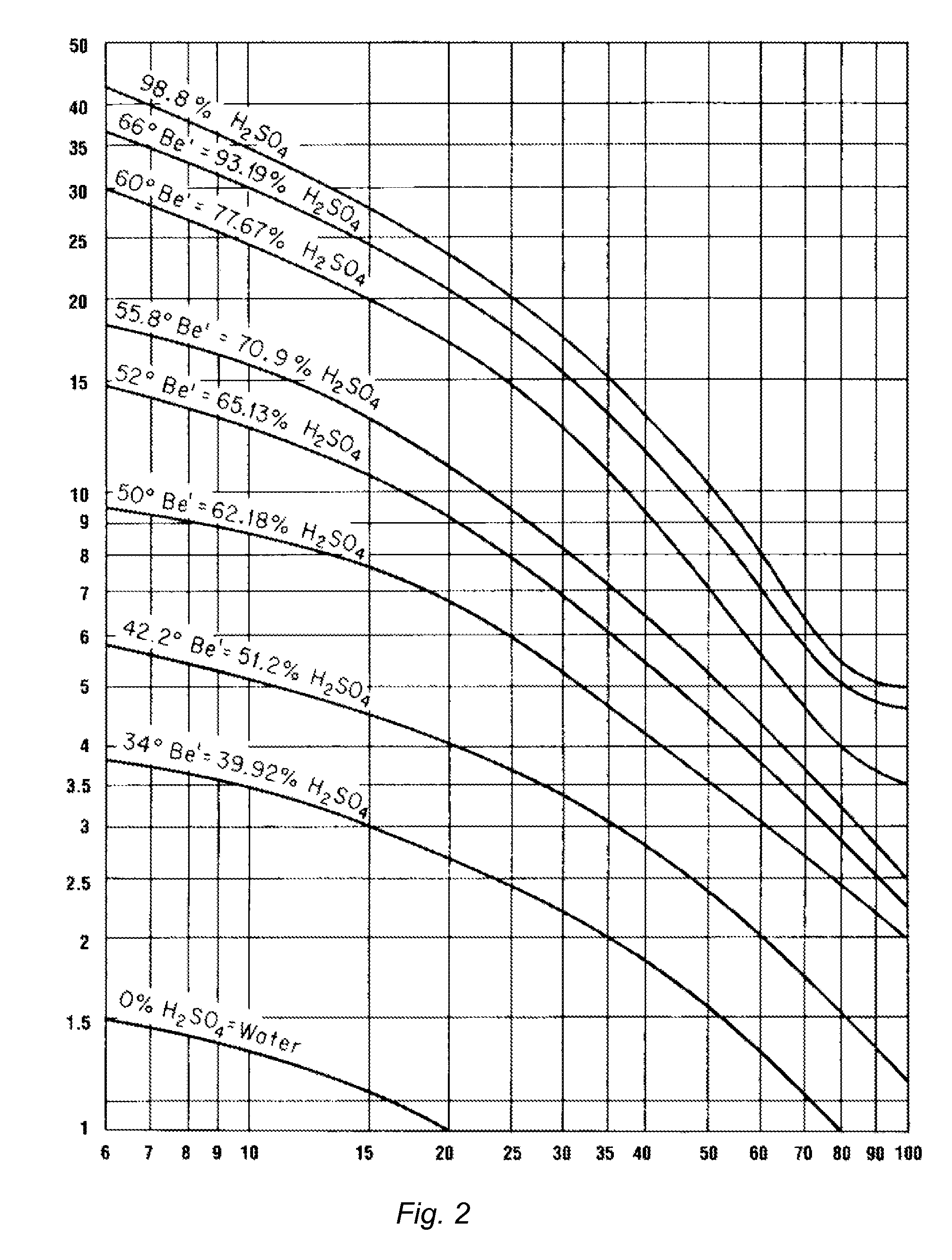
[0019]In FIG. 2 sulfuric acid solutions are again shown, with the ordinate again being viscosity in cP but with those of the abscissa now being temperature in ° C. and the curves indicating various concentrations.

[0020]The present inventors have discovered that such liquids can be much more quickly re...


PUM

PropertyMeasurementUnit
Temperatureaaaaaaaaaa
Fractionaaaaaaaaaa
Fractionaaaaaaaaaa

Abstract

Mixtures containing concentrated sulfuric acid used for stripping photoresist from semiconductor wafer, such as SOM and SPM mixtures, are more quickly removed from a wafer surface using another liquid also containing high concentration of sulfuric acid, with the second liquid furthermore containing controlled small amounts of fluoride ion. The second liquid renders the wafer surface hydrophobic, which permits easy removal of the sulfuric acid therefrom by spinning and / or rinsing.

Description

BACKGROUND OF THE INVENTION[0001]1. Field of the Invention[0002]The invention relates to processes for treating disc-shaped articles such as semiconductor wafers and glass wafers, and especially to processes for cleaning surfaces of semiconductor wafers.[0003]2. Description of Related Art[0004]Semiconductor wafers undergo a variety of wet processing stages during manufacture of integrated circuits, such as removal of photoresist from the wafer. When the photoresist is stripped by a wet process, typically a strong inorganic acid is used at high concentration, with sulfuric acid being most prevalent. Among the chemical compositions used for that stripping are solutions of sulfuric acid mixed with hydrogen peroxide (SPM) and mixtures of ozone and sulfuric acid (SOM). Also mixtures of sulfuric acid with hydrogen peroxide and ozone (SPOM) are being sometimes used.[0005]The cleaning solution or mixture including a high concentration of strong inorganic acid must then itself be removed fro...

Claims


Application Information

Patent Timeline
IPC IPC(8): B08B3/00
CPCC03C23/0075C11D7/08C11D11/0035H01L21/02057C11D11/0064H01L21/02052C11D11/0047C11D2111/18C11D2111/44C11D2111/22C11D1/02H01L21/02C11D1/22
Inventor OKORN-SCHMIDT, HARALDFRANK, DIETERKUMNIG, FRANZ
Owner LAM RES AG
Learn More