Electroplating method

a technology of electroplating and film filling, which is applied in the direction of sealing devices, contact devices, coatings, etc., can solve the problems of time required, difficulty in attempting to meet ideal requirements, and conventional electroplating processes have failed to achieve both ideal filling of plated films, etc., and achieve the effect of shortening the time required

Inactive Publication Date: 2012-06-28
EBARA CORP
View PDF7 Cites 16 Cited by
  • Summary
  • Abstract
  • Description
  • Claims
  • Application Information

AI Technical Summary

Benefits of technology

[0024]According to the present invention, as described above, the plural plating processes are performed, each for a predetermined period, on the face and reverse sides of the substrate by supplying pulsed currents respectively between the face side of the substrate and one of the anodes which faces the face side of the substrate, and between the reverse side of the substrate and the other of the anodes which faces the reverse side of the substrate. Accordingly, it is possible to fill a plated

Problems solved by technology

However, it is generally practically difficult to attempt to meet the ideal requirements and at the same time to fill the plated film efficiently into the through-hole to shorten the time required to perform the plating process.
Stated otherwise, t

Method used


Image

  • Electroplating method
  • Electroplating method
  • Electroplating method

Examples


Embodiment Construction

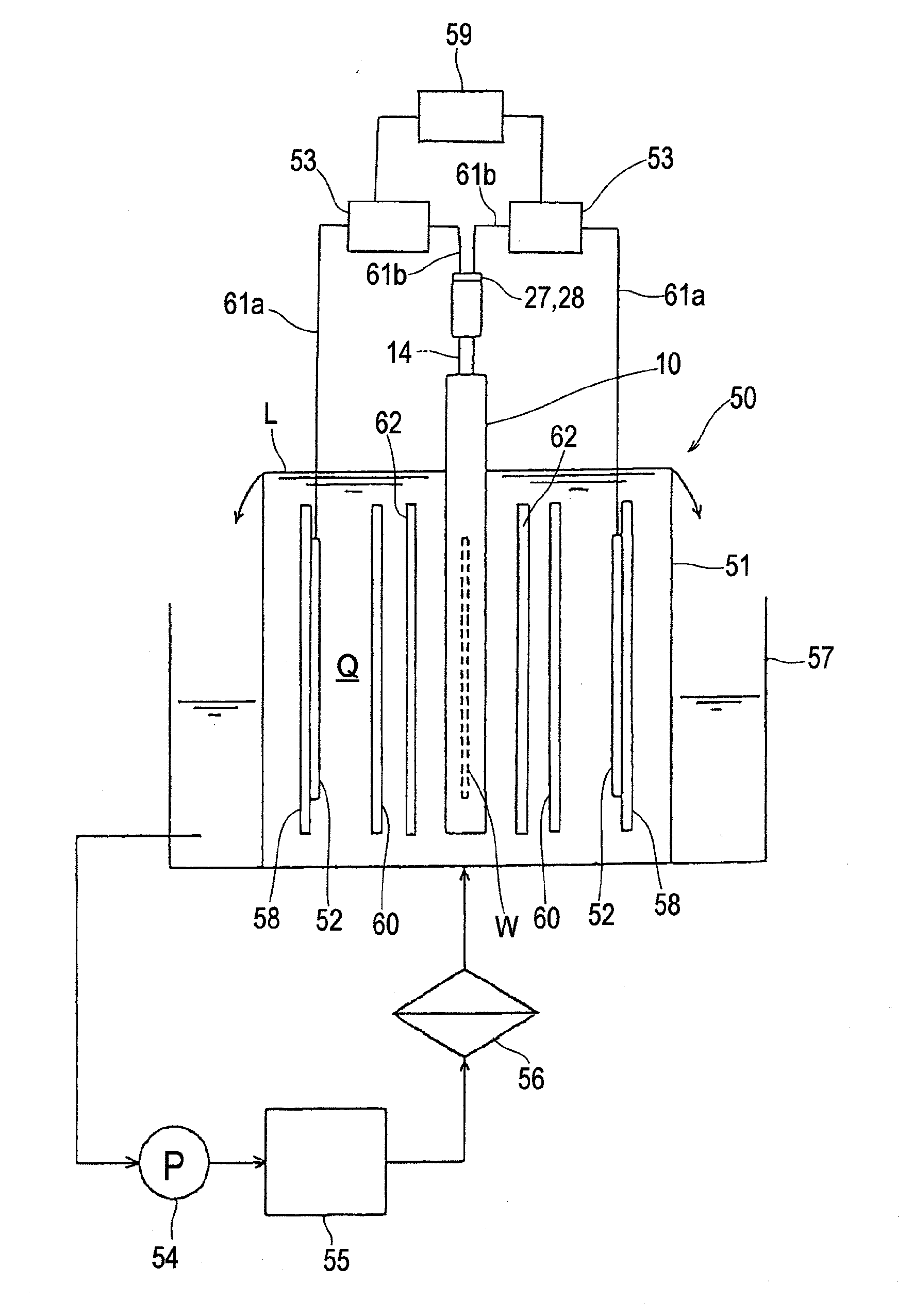
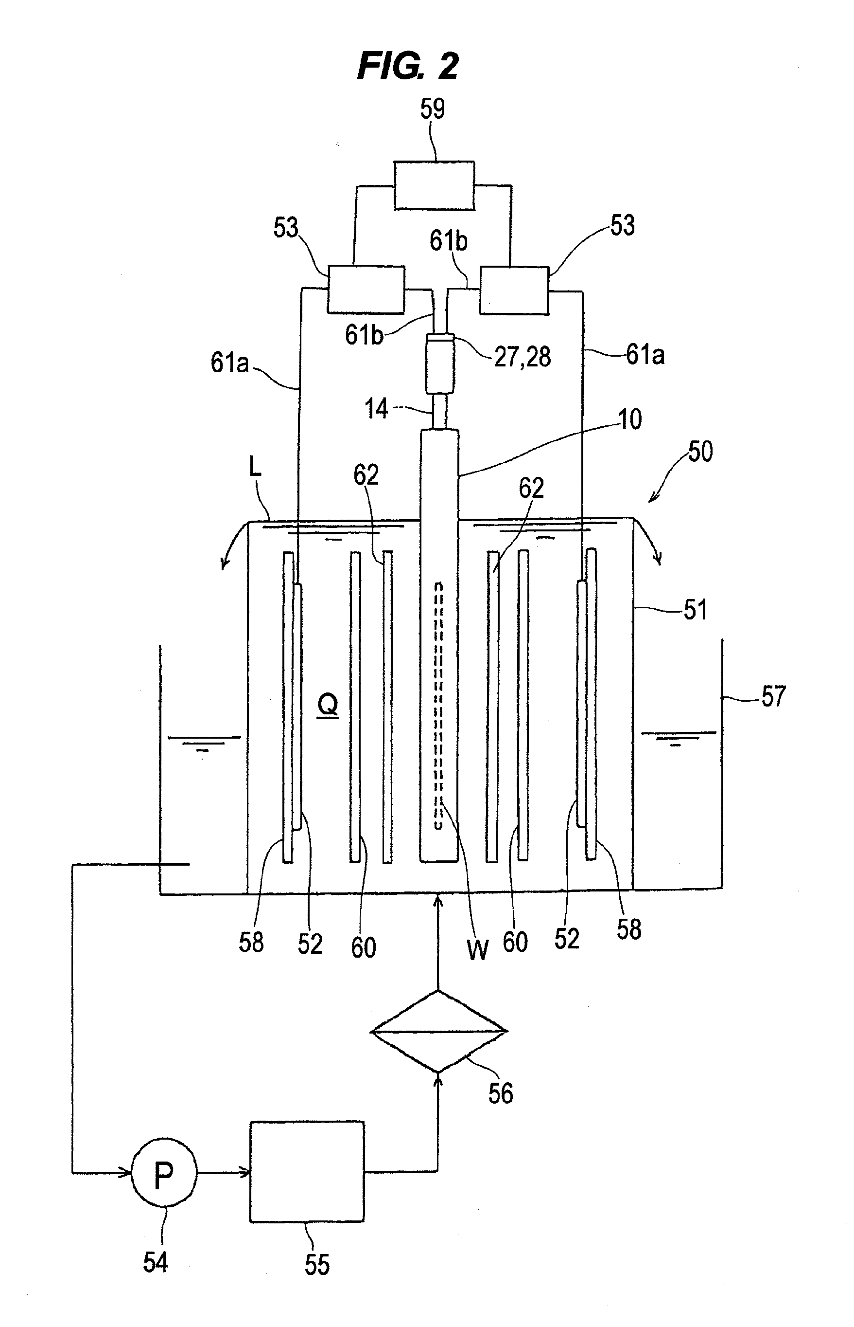
[0058]Preferred embodiments of the present invention will now be described with reference to the drawings. FIG. 2 is a vertical sectional front view schematically showing an electroplating apparatus 50 which is used to carry out an electroplating method according to the present invention. As shown in FIG. 2, the electroplating apparatus 50 includes a plating tank 51 holding a plating solution Q therein, and a substrate holder 10 holding a substrate W such as a semiconductor wafer or the like and suspended vertically in the plating solution Q. The plating solution Q with the substrate holder 10 immersed therein has a surface level L at the upper end of the plating tank 51, as shown in FIG. 2. Two insoluble anodes 52 supported on respective anode holders 58 are disposed in the plating tank 51 in facing relation to respective opposite surfaces, i.e., face and reverse sides, of the substrate W held by the substrate holder 10. As shown in FIG. 3, the substrate holder 10 includes a first ...


PUM

PropertyMeasurementUnit
Currentaaaaaaaaaa
Current densityaaaaaaaaaa

Abstract

A substrate with a through-hole is immersed in a plating solution in a plating tank. A pair of anodes are disposed in the plating solution in the plating tank in facing relation to face and reverse sides, respectively, of the substrate in the plating solution. A plurality of plating processes are performed on the face and reverse sides by supplying pulsed currents respectively between the face side of the substrate and one of the anodes which faces the face side of the substrate, and between the reverse side of the substrate and the other anode which faces the reverse side of the substrate. A reverse electrolyzing process is performed on the face and reverse sides between adjacent plating processes by supplying currents in an opposite direction to the pulsed currents respectively between the face side of the substrate and one of the anodes, and between the reverse side of the substrate and the other anode.

Description

BACKGROUND OF THE INVENTION[0001]1. Field of the Invention[0002]The present invention relates to an electroplating method for simultaneously plating both the face and reverse sides of a substrate which has a through-hole vertically penetrating in its interior to fill a plated film of metal such as copper or the like into the through-hole.[0003]2. Description of the Related Art[0004]A technique of forming a plurality of through-vias of a metal, vertically penetrating through a substrate, is known as a method to electrically connect the layers of a multi-layer stack of substrates such as semiconductor substrates. It is customary to make vertical through-vias in a substrate by simultaneously plating both the face and reverse sides of a substrate, which has through-holes vertically penetrating in its interior, thereby to fill a plated film of metal into the through-holes.[0005]There is known an electroplating apparatus for producing through-vias (see Japanese Patent No. 4138542). This e...

Claims


Application Information

Patent Timeline
IPC IPC(8): C25D5/18C25D11/02
CPCC25D11/024C25D5/18H01L21/76898H01L21/2885C25D7/123C25D17/08C25D17/005C25D17/004C25D17/001
Inventor ARAKI, YUJISAITO, NOBUTOSHIFUJIKATA, JUMPEI
Owner EBARA CORP
Why Eureka
Try Eureka