Thin-Film Antenna

Inactive Publication Date: 2012-06-28
ADVANCED CONNECTEK INC
View PDF3 Cites 0 Cited by
  • Summary
  • Abstract
  • Description
  • Claims
  • Application Information

AI Technical Summary

Benefits of technology

[0007]Another objective of the present invention is to provide a thin-film antenna, wherein a flexible radiation conductor replaces a rigid one to reduce the overall thickness of a product, and wherein a conductive metallic thimble of a conduction member is used to prevent the thin-film flexible radiation conductor from protruding or breaking, whereby is decreased the fabrication cost and promoted the yield rate.
[0009]The present invention is characterized in replacing the conventional rigid metallic radiation conductor with a thin-film flexible radiation conductor. The flexible radiation conductor is fabricated via using a photolithographic process and an etching process to form a pattern of the flexible radiation conductor on a soft substrate, and extending the substrate into a 3D shape at high temperature and under high pressure. Thereby, the flexible radiation conductor has superior pliability and bendability. The finished flexible radiation conductor can be stuck onto an arbitrary surface of an object, such as a complicated surface or a curved surface. Alternatively, the finished flexible radiation conductor is disposed inside an injection mold beforehand, and then embedded in a plastic member via injection molding.
[0010]Via replacing the conventional rigid metallic radiation conductor with a thin-film flexible radiation conductor and disposing the thin-film flexible radiation conductor on a surface of an accommodation space of a plastic member, the present invention can greatly reduce the overall thickness of a product. Further, the present invention uses a conductive metallic thimble of a conduction member to prevent the thin-film radiation conductor from protruding or breaking. Thereby is promoted the yield rate of products.

Problems solved by technology

Such a requirement makes the realization of a multiband system more complicated.
Therefore, the appearance design and integration capability of a multiband antenna become a big challenge.
However, when the contact terminals conducting electric signals are inserted into the holes of a plastic housing in the practical fabrication process, they are likely to bump the radiation conductors and the thin film because the operator is hard to control the inserting force.
Thus, the radiation conductors may be damaged, and the thin film may be bulged.
Then, the antenna may malfunction.

Method used


Image

  • Thin-Film Antenna
  • Thin-Film Antenna
  • Thin-Film Antenna

Examples


first embodiment

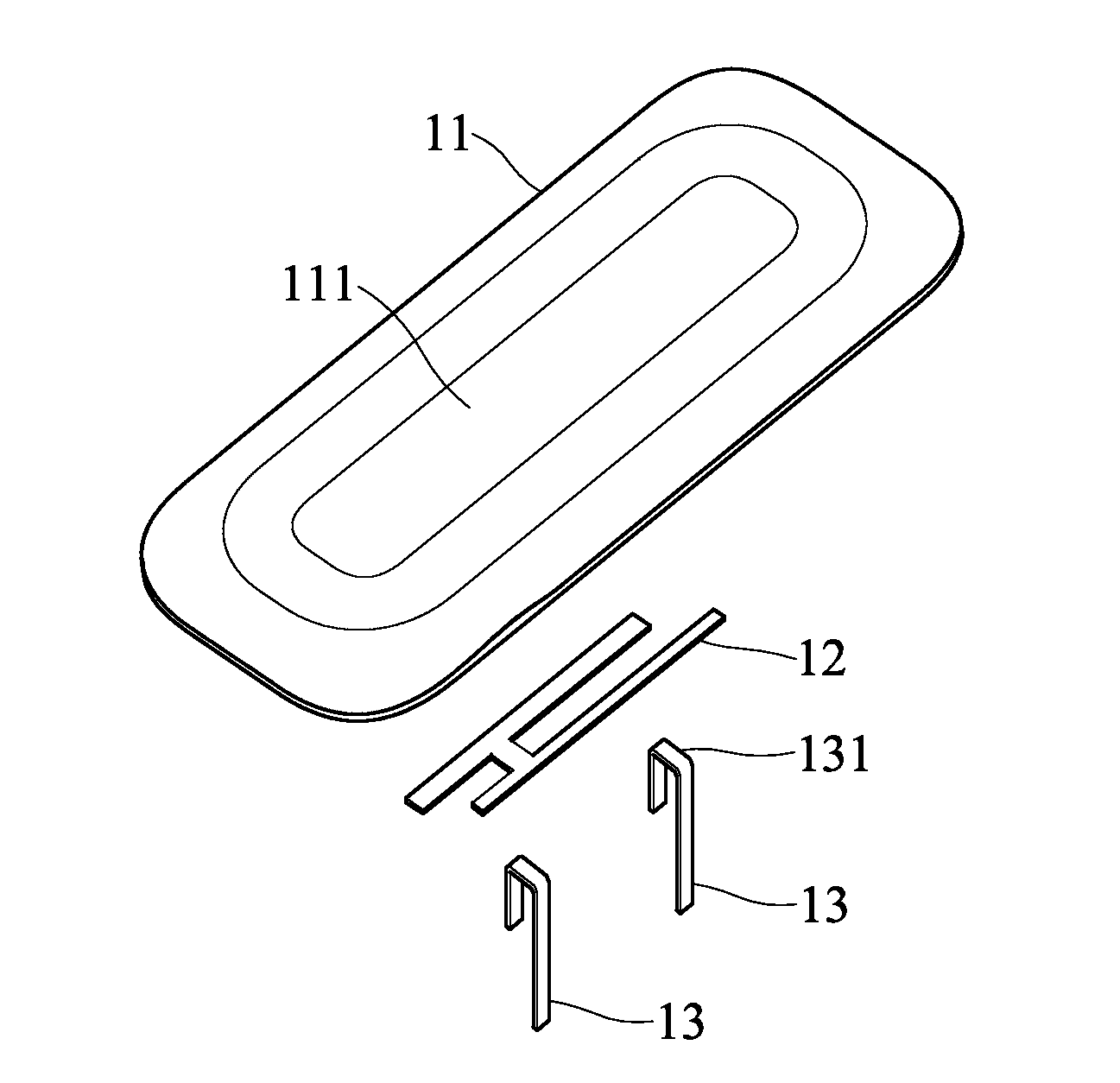
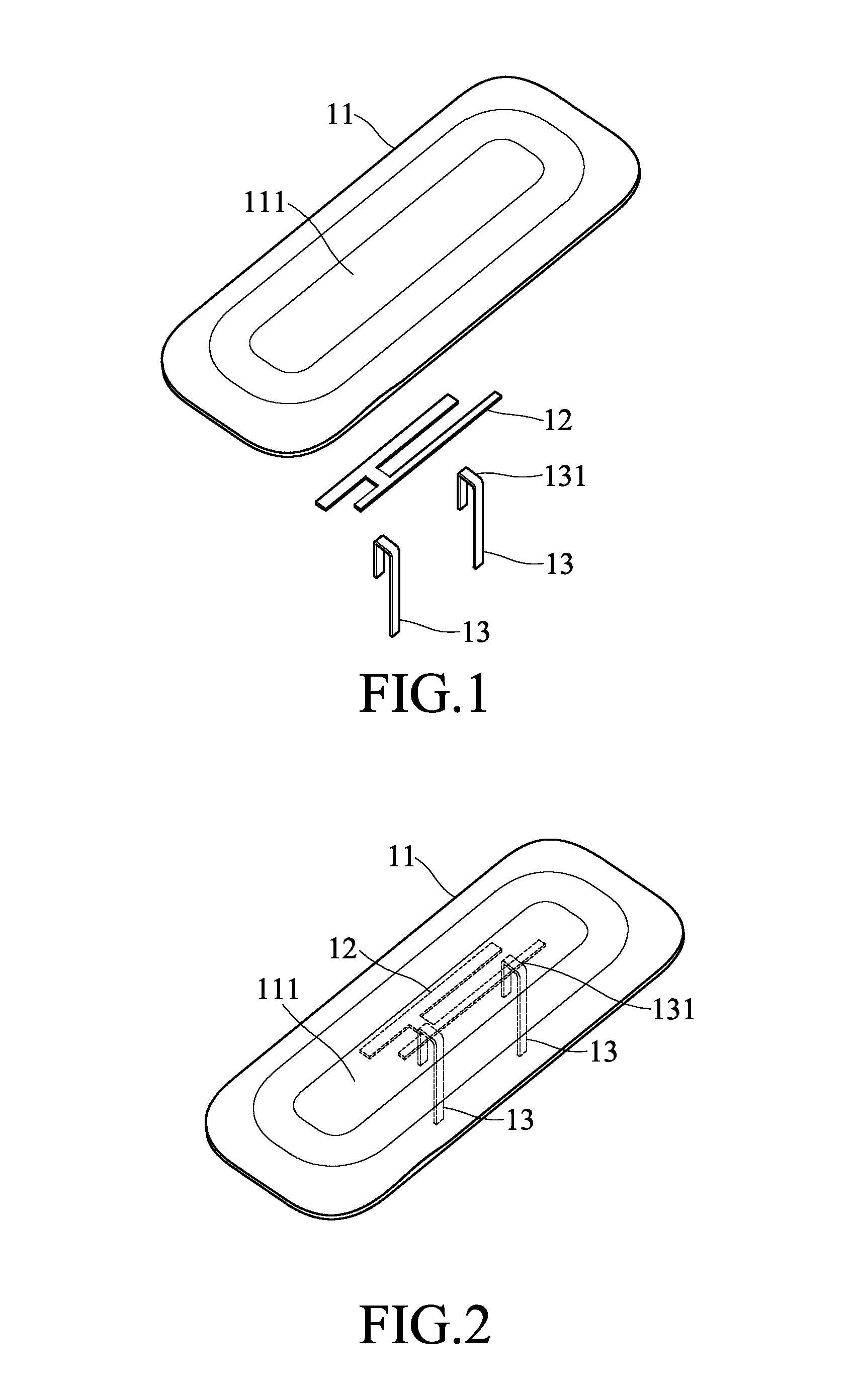
[0023]In the first embodiment, the plastic member 11 has an about rectangular shape with a length of about 70 mm, a width of about 28 mm, and a thickness of about 0.05 mm. The accommodation space 111 is located at the center of the plastic member 11 and has a length of about 40 mm and a width of about 8 mm. The flexible conductor 12 has an H-like shape. The rectangle of the H-like shape, which does not contact the conduction member 13, has a length of about 24 mm, a width of about 2 mm and a thickness of about 0.02 mm. The rectangle of the H-like shape, which contacts the conduction member 13, has a length of 28 mm, a width of about 1.5 mm and a thickness of about 0.02 mm. The middle rectangle of the H-like shape has a length of about 3 mm, a width of about 2 mm and a thickness of about 0.02 mm. The conduction member 13 has a J-like shape. The long rectangle of the J-like shape has a length of about 8 mm and a width of about 2 mm. The short rectangle of the J-like shape has a length...

second embodiment

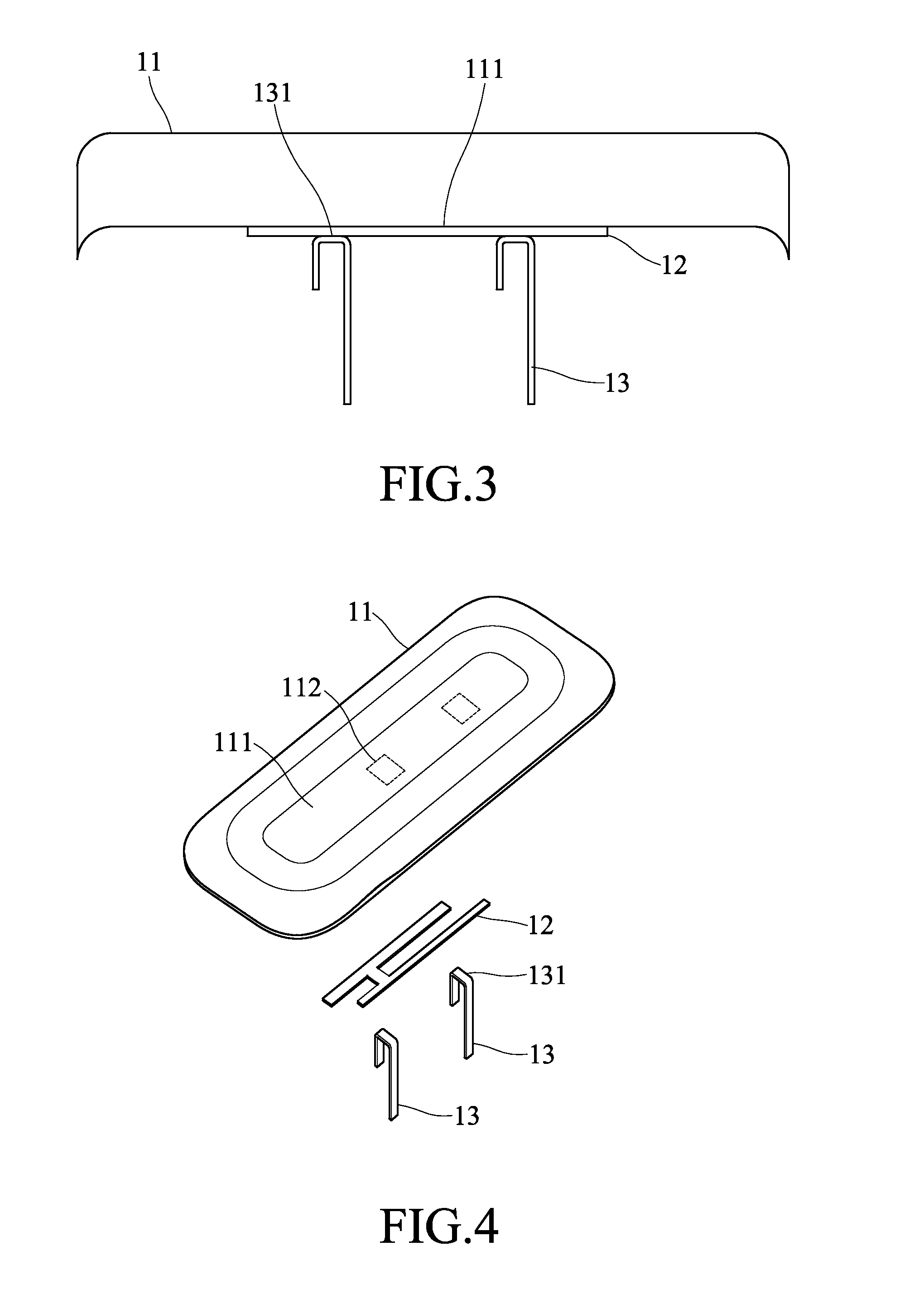
[0026]Refer to FIG. 6 a side view of the thin-film antenna according to the present invention. The flexible antenna 12 is arranged inside an injection mold beforehand and completely airtightly embedded on the inner surface of the plastic member 11 after injection molding. The through-hole 112 is pre-stamped in the plastic member 12, allowing the contact terminal 131 of the conduction member 13 to penetrate the plastic member 13 and physically contact the flexible radiation conductor 12. Thereby, electric signals can be conducted by the thimble of the conduction member 13.

[0027]Refer to FIG. 7 a side view of a thin-film antenna according to a third embodiment of the present invention. The third embodiment is basically similar to the first embodiment but different from the first embodiment in that the flexible radiation conductor 12 is embedded on upper outer surface of the accommodation space 111 of the plastic member 11. After having been stuck onto the upper outer surface of the pl...


PUM


Abstract

A thin-film antenna comprises a plastic member, a flexible radiation conductor and a conduction member. The plastic member has an accommodation space. The flexible radiation conductor is disposed on one surface of the accommodation space. The conduction member has a contact terminal physically contacting the flexible radiation conductor. The flexible radiation conductor is embedded on one surface of the accommodation space of the plastic housing of a wireless communication device via a hot pressing process. The flexible radiation conductor can replace the conventional complicated rigid metallic radiation conductor to reduce thickness of products. The conduction member has a conductive metallic thimble for conducting electric signals, which can prevent the thin-film radiation conductor from protruding or breaking. The superior pliability and bendability of the flexible radiation conductor enables the flexible radiation conductor to integrate with an arbitrary surface, such as a complicated surface or a curved surface.

Description

BACKGROUND OF THE INVENTION[0001]1. Field of the Invention[0002]The present invention relates to a thin-film antenna, particularly to an antenna having a thin-film flexible radiation conductor.[0003]2. Description of the Related Art[0004]The embedded antenna has evolved from a single and narrow band system to a multi and broad band system. The elements of a multiband system should be miniaturized as much as possible. Such a requirement makes the realization of a multiband system more complicated. The consumers have a bias for wireless communication devices with a smooth and neat appearance. Therefore, the appearance design and integration capability of a multiband antenna become a big challenge.[0005]However, when the contact terminals conducting electric signals are inserted into the holes of a plastic housing in the practical fabrication process, they are likely to bump the radiation conductors and the thin film because the operator is hard to control the inserting force. Thus, th...

Claims


Application Information

Patent Timeline
IPC IPC(8): H01Q1/38
CPCH01Q1/40H01Q1/38
Inventor TSUNG-WEN, CHIUFU-REN, HSIAOPO-SHENG, CHEN
Owner ADVANCED CONNECTEK INC
Why Eureka
Try Eureka