Semiconductor light-emitting diode and a production method therefor

a technology of light-emitting diodes and semiconductors, applied in the direction of semiconductor/solid-state device manufacturing, semiconductor devices, electrical apparatus, etc., can solve the problems of thermal stability degradation upon high output, need to be improved, and the light output of conventional nitride-based leds is not satisfactory, so as to achieve excellent ohmic characteristics, less degradation of ohmic characteristics, and excellent thermal stability

Active Publication Date: 2012-07-05
SEOUL VIOSYS CO LTD +1
View PDF0 Cites 25 Cited by
  • Summary
  • Abstract
  • Description
  • Claims
  • Application Information

AI Technical Summary

Benefits of technology

[0010]The present invention is directed to solving such problems, and provides a semiconductor light emitting diode and a method of manufacturing the same, which has excellent thermal stability to undergo less degradation of ohmic characteristics in a high temperature environment and includes ohmic electrodes having excellent ohmic characteristics not only at a Ga-face of a nitride semiconductor layer, but also at an N-face thereof.
[0025]In an ohmic electrode of a multilayer structure including a nanodot layer / a contact layer / an anti-diffusion layer / a capping layer according to some embodiments, the nanodot layer is formed on an N-face of a nitride semiconductor and provides excellent ohmic characteristics through improvement of charge injection characteristics, and the contact layer acts as a diffusion barrier and suppresses degradation by heat generated under conditions for annealing in a nitrogen atmosphere, high temperature, and high current injection, thereby providing excellent thermal stability.
[0026]In addition, the ohmic electrode of the multilayer structure including the nanodot layer / the contact layer / the reflective layer / the anti-diffusion layer / the capping layer according to the embodiments may have excellent reflectivity, thereby preventing degradation in light output caused by absorption of light, and may exhibit excellent ohmic characteristics without separate annealing, thereby enabling high output through application of high electric current.

Problems solved by technology

However, conventional nitride-based LEDs are not satisfactory in terms of light output, luminous efficacy and price, and need improved performance.
Since such a lateral type light emitting diode may be manufactured through a relatively simple process, it is advantageous in terms of low manufacturing cost, but the use of the sapphire substrate which is an insulator and exhibits low thermal conductivity leads to degradation in thermal stability upon high output and heat accumulation through application of electric current to large area.
At this time, it is difficult to perform annealing at high temperature after laser lift-off due to wafer bonding temperature and large difference in thermal expansion coefficients between the metal substrate and a GaN layer.
However, such ohmic electrodes have a problem in that ohmic characteristics are easily deteriorated causing increase in operating voltage by heat generated during annealing for formation of a SiO2 protective layer after formation of the electrodes or during injection of high electric current in a large area light emitting diode.
Further, the Ti / Al electrode has problems in that Al can be easily oxidized and the Ti / Al electrode can be easily etched by various kinds of solutions.
However, since a general n-type electrode such as a Cr / Au or Ti / Al electrode uses a thick Cr or Ti layer having low reflectivity, part of the n-type electrode absorbing light from the active layer increases with increasing area of the n-type electrode, causing obstruction against improvement of light output.
However, unlike the Ga-face, it is difficult to obtain good ohmic characteristics with the N-face without annealing and the difference in thermal expansion coefficients between the assistant substrate (metal substrate) and the nitride semiconductor layer makes it difficult to perform annealing itself.
As such, a conventional Cr / Au or Ti / Al electrode formed on the N-face exhibits undesired ohmic characteristics and has low thermal stability.

Method used


Image

  • Semiconductor light-emitting diode and a production method therefor
  • Semiconductor light-emitting diode and a production method therefor
  • Semiconductor light-emitting diode and a production method therefor

Examples


embodiment 1

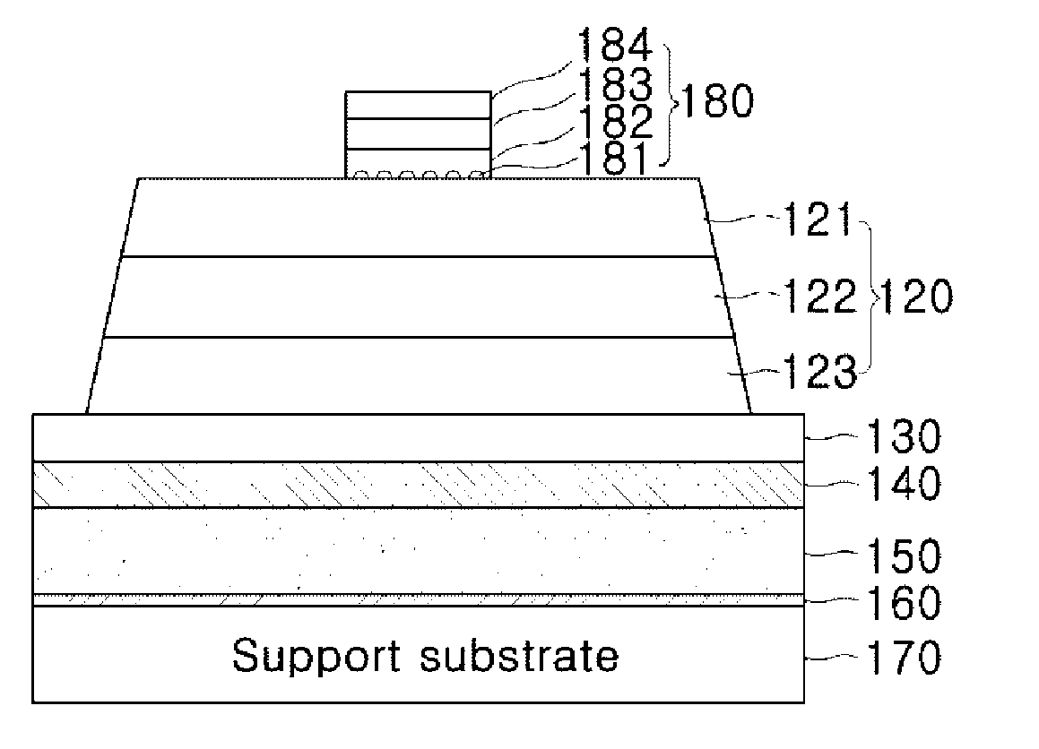
[0044]FIG. 1 is a sectional view of a semiconductor light emitting diode according to a first embodiment of the present invention.

[0045]Referring to FIG. 1, the semiconductor light emitting diode according to the first embodiment includes: a semiconductor layer 120, which includes an n-type layer 121, an active layer 122, and a p-type layer 123; an n-type electrode 180 formed on an upper surface of the n-type layer 121; and a p-type electrode 130 formed on a lower surface of the p-type layer 123. The semiconductor light emitting diode may further include a support substrate 170 attached to a lower surface of the p-type electrode 130. Here, the n-type electrode 180 is an ohmic electrode of a multilayer structure, which includes a nanodot layer 181, a contact layer 182, an anti-diffusion layer 183 and a capping layer 184 formed on the semiconductor layer 120 and is in ohmic contact with the semiconductor layer 120.

[0046]The semiconductor layer 120 includes the n-type layer 121, the ac...

embodiment 2

[0070]FIG. 9 is a sectional view of a semiconductor light emitting diode according to a second embodiment of the present invention.

[0071]Referring to FIG. 9, the semiconductor light emitting diode according to the second embodiment includes: a semiconductor layer 120, which includes an n-type layer 121, an active layer 122, and a p-type layer 123; an n-type electrode 1180 formed on an upper surface of the n-type layer 121; and a p-type electrode 130 formed on a lower surface of the p-type layer 123. The semiconductor light emitting diode further includes a support substrate 170 attached to a lower surface of the p-type electrode 130 to support the entire structures 120, 130, 1180. Here, the n-type electrode 1180 is an ohmic electrode of a multilayer structure, which includes a nanodot layer 1181, a contact layer 1182, a reflective layer 1183, an anti-diffusion layer 1184 and a capping layer 1185 formed on the semiconductor layer 120 and is in ohmic contact with the semiconductor lay...

embodiment 3

[0087]The ohmic electrode of the Ag nanodot layer / Ti / Cr / Au structure according to the present invention may also be applied to a lateral type semiconductor light emitting diode. Next, a semiconductor light emitting diode according to a third embodiment, in which an n-type electrode and a p-type electrode are disposed in a lateral structure, will be described. Here, a repetitive description will be omitted or will be described in brief.

[0088]FIG. 13 is a sectional view of, the semiconductor light emitting diode according to the third embodiment of the present invention.

[0089]Referring to FIG. 13, the semiconductor light emitting diode according to the third embodiment includes a semiconductor layer 220, which includes an n-type layer 221, an active layer 222, and a p-type layer 223 sequentially formed on a substrate 210; an n-type electrode 230 formed on an exposed region of the n-type layer 221; and a p-type electrode 240 formed on the p-type layer 223. Here, at least one of the n-t...


PUM


Abstract

Provided is a semiconductor light-emitting diode including a semiconductor layer having a light-emitting structure; and an ohmic electrode incorporating a nanodot layer, a contact layer, a diffusion-preventing layer and a capping layer on the semiconductor layer. The nanodot layer is formed on the N-polar surface of the semiconductor layer and is formed from a substance comprising at least one of Ag, Al and Au. Also provided is a production method therefor. In the ohmic electrode which has the multi-layer structure comprising the nanodot layer / contact layer / diffusion-preventing layer / capping layer in the semiconductor light-emitting diode of this type, the nanodot layer constitutes the N-polar surface of a nitride semiconductor and improves the charge-injection characteristics such that outstanding ohmic characteristics can be obtained.

Description

CROSS-REFERENCE RELATED APPLICATIONS[0001]This application is the National Stage Entry of International Application PCT / KR2010 / 006056, filed on Sep. 7, 2010, and claims priority from and the benefit of Korean Patent Application Nos. 10-2009-0084086, filed on Sep. 7, 2009, and 10-2009-0084087, filed on Sep. 7, 2009, all of which are herein incorporated by reference for all purposes as if fully set forth herein.FIELD OF THE INVENTION[0002]The present invention relates to a semiconductor light emitting diode and a method of manufacturing the same, and more particularly, to a semiconductor light emitting diode and a method of manufacturing the same, which includes an ohmic electrode formed on a semiconductor layer of a light emitting structure and used for application of an external power source.DISCUSSION OF THE BACKGROUND[0003]A semiconductor light emitting diode (LED) has a long lifespan, permits a reduction in size and weight, exhibits strong orientation of light, and can be operate...

Claims


Application Information

Patent Timeline
Patent Type & Authority Applications(United States)
IPC IPC(8): H01L33/60H01L33/62
CPCH01L33/0095H01L33/40H01L33/387H01L33/32
Inventor LEE, JONG LAMSONG, YANG HEESON, JUN HOKIM, BUEM JOON
Owner SEOUL VIOSYS CO LTD
Why Eureka
Try Eureka