Touchable sensing matrix unit, a co-constructed active array substrate having the touchable sensing matrix unit and a display having the co-constructed active array substrate

a technology of touchable sensing and matrix unit, which is applied in the field of active array display, can solve the problems of affecting the transmittance of the flat panel display, nothing but, lowering yield, and higher production cost, and achieve the effect of facilitating writing

Inactive Publication Date: 2012-07-05
LIU HUNG TA
View PDF2 Cites 43 Cited by
  • Summary
  • Abstract
  • Description
  • Claims
  • Application Information

AI Technical Summary

Benefits of technology

[0013]An objective of the present invention is to provide a display device having a touchable sensing matrix unit formed on a co-constructed active array substrate.
[0002]The present invention relates to an active-array display having an integrated touch control function and more particularly to a touchable sensing matrix unit mounted on a co-constructed active array substrate, having lead wires including multiple first sensing and transmitting circuits and multiple second sensing and transmitting circuits angularly intersecting with each other, and being conductive and cyclic.

Problems solved by technology

However, being too thick is the drawback of such structural design and affects transmittance of the flat panel display 90.
Once the production processes and structures of the display device are altered, challenges encountered first are nothing but lowered yield and higher production cost.
Additionally, each pixel electrode of the TFT array substrate further needs two metal pads, X-axis and Y-axis auxiliary circuits, thereby not only reducing a visible area of the pixel electrode but also making the production processes of the TFT array substrate complicated.
Moreover, pressure and deformation sensed at the center, edges and corners of the pixel display area of a glass substrate all differ from one another while the sensed pressure is uneasy to be calibrated.
More importantly is that multi-touch sensing is unavailable in such type of touch panels, and such unavailability is a major technical issue.
The production processes must be also altered, and the production processes are more complicated and the production cost significantly increases.

Method used


Image

  • Touchable sensing matrix unit, a co-constructed active array substrate having the touchable sensing matrix unit and a display having the co-constructed active array substrate
  • Touchable sensing matrix unit, a co-constructed active array substrate having the touchable sensing matrix unit and a display having the co-constructed active array substrate
  • Touchable sensing matrix unit, a co-constructed active array substrate having the touchable sensing matrix unit and a display having the co-constructed active array substrate

Examples


case 1

[0071] Active Array TFT LCD Display (I)

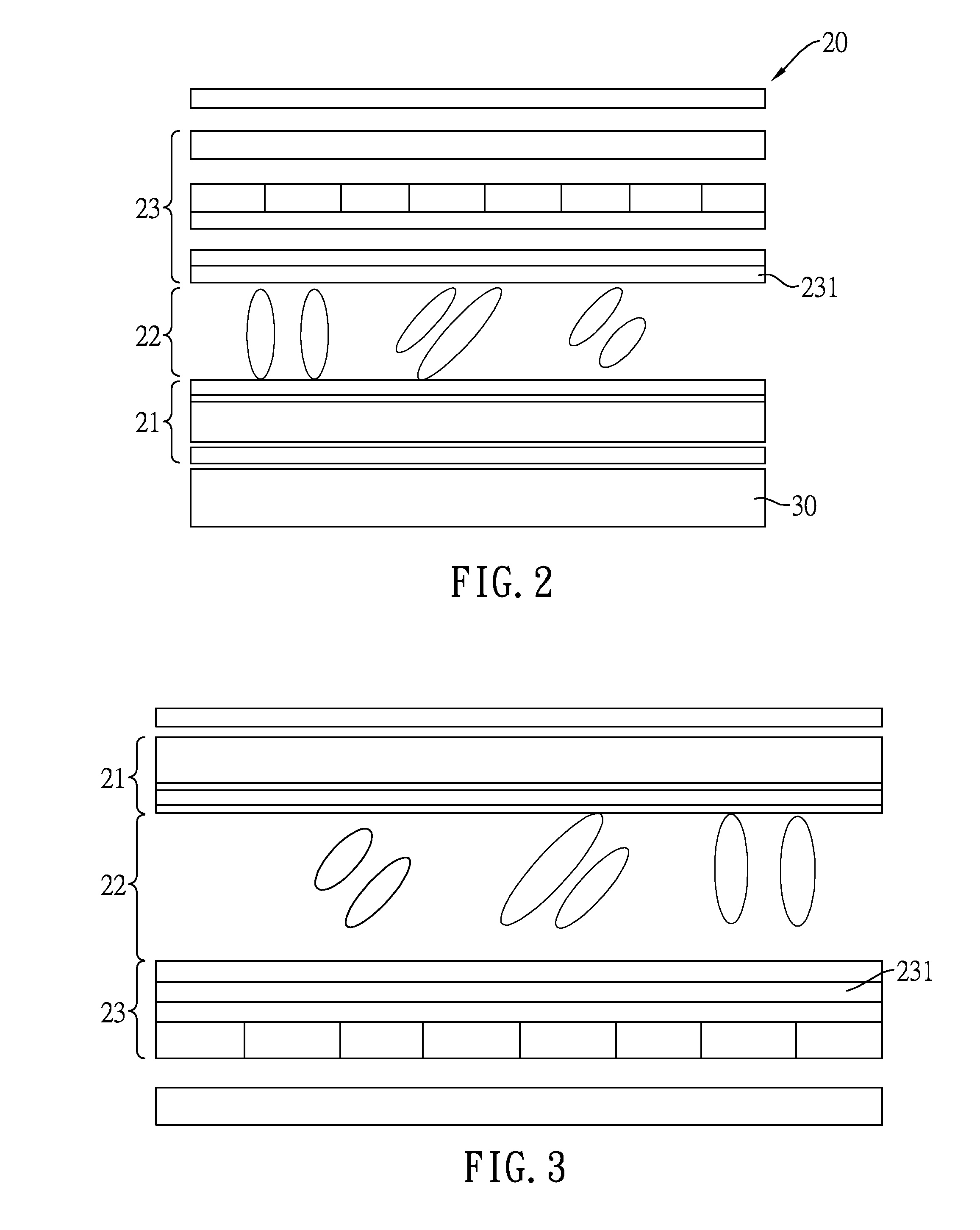
[0072]With reference to FIG. 2, an active array TFT LCD display or flat panel display may be one of transmissive, reflective and transflective TFT LCD display or low-temperature poly-Si (LTPS) TFT displays, or an LcoS formed by micro-pixel array on semiconductor chips. The active array TFT LCD display at least has an upper substrate 23, a lower active array substrate 21 and a liquid crystal layer 22. The upper substrate 23 may be a color filter substrate and has a common electrode 231 formed thereon. The lower active array substrate 21 is a co-constructed active array substrate. The liquid crystal layer 22 is mounted between the upper substrate 23 and the lower active array substrate 21. In the case of a transmissive display, the active array TFT LCD display further has a backlight module 30 mounted on a bottom thereof. If considering that electrode signals of the common electrode 231 possibly mask capacitive sensing signals, the present case i...

case 2

[0073] Active Array TFT LCD Display (II)

[0074]In the present case, with reference to FIG. 3, the active array TFT LCD display or flat panel display may be a transmissive TFT LCD display or an LTPS TFT LCD display, and at least has an upper active array substrate 21, a lower color filter substrate 23 and a liquid crystal layer 22. The upper active array substrate 21 is a co-constructed active array substrate. The liquid crystal layer 22 is mounted between the upper active array substrate 21 and the lower color filter substrate 23. The first and second sensing and transmitting wires of the touchable sensing matrix unit in accordance with the present invention are data lines and scan lines formed on an active array substrate of the upper active array substrate 21. According to the design of the co-constructed active array substrate, the first or second sensing and transmitting circuit of the touchable sensing matrix unit may be implemented and co-constructed by signal lines, read lines...

case 3

[0076] Active Array TFT LCD Display of Flat Panel Display Similar to that in Case 1

[0077]With reference to FIG. 5, a fringe field switching wide viewing angle TFT LCD display at least has a lower active array substrate 21, an upper substrate 23′, a polarizer 24 and a liquid crystal molecule layer 22 mounted between the lower active array substrate 21 and the upper substrate 23′. The lower active array substrate 21 has a first substrate 211, a pixel layer 212 and a common electrode layer 213. The pixel layer 212 and the common electrode layer 213 are sequentially formed on one side of the first substrate 211 and the structure thereof has a fringe field design as shown by the common electrode layers 213 in FIG. 6, and each two common electrode layers 213 are separated by an insulation layer. The active array TFT LCD display in the present case may further have a color filter layer 232 mounted on the substrate 231 of the upper substrate 23′ while containing no common electrodes. The fi...


PUM

PropertyMeasurementUnit
conductiveaaaaaaaaaa
positive dielectricaaaaaaaaaa
transmittanceaaaaaaaaaa

Abstract

The present invention relates to a touchable sensing matrix unit, a co-constructed active array substrate having the touchable sensing matrix unit and a display having the co-constructed active array substrate. The touchable sensing matrix unit is formed on the co-constructed active array substrate and has multiple first sensing and transmitting wires and multiple second sensing and transmitting wires. The first and second sensing and transmitting wires are conductive and cyclic, intersect to form an angle, and sandwich an insulation layer formed therebetween. The touchable sensing matrix unit has at least one set of wires of the co-constructed active array substrate and an improved design using the at least one set of wires.

Description

BACKGROUND OF THE INVENTION[0001]1. Field of the Invention[0002]The present invention relates to an active-array display having an integrated touch control function and more particularly to a touchable sensing matrix unit mounted on a co-constructed active array substrate, having lead wires including multiple first sensing and transmitting circuits and multiple second sensing and transmitting circuits angularly intersecting with each other, and being conductive and cyclic.[0003]2. Description of the Related Art[0004]High yield and accurate touch control of touch panels is attributable to advanced development of the touch panels. Touch panels can be classified into electromagnetic, resistive, capacitive, optical (infrared and SAW) types and the like.[0005]To facilitate users' input, a light, thin and compact electronic product usually addresses a space-saving approach providing a touch panel stacked on a display screen thereof. With reference to FIG. 25, a touch panel 91 is mounted o...

Claims


Application Information

Patent Timeline
Patent Type & Authority Applications(United States)
IPC IPC(8): G06F3/041G02F1/1368
CPCG06F3/0412G06F3/0416G06F2203/04106G06F3/044G06F3/046G06F3/042G06F3/04166G06F3/0445G06F3/0446
Inventor LIU, HUNG-TA
Owner LIU HUNG TA
Why Eureka
Try Eureka