Method for manufacturing a polycrystalline dielectric layer

a technology of polycrystalline dielectric and manufacturing method, which is applied in the direction of chemical vapor deposition coating, coating, electrical equipment, etc., can solve the problems of lowering the final crystallization rate of the zrosub>2 /sub>layer, difficult crystalline growth of a dielectric material, and extremely detrimental effects

Active Publication Date: 2012-07-05
STMICROELECTRONICS (CROLLES 2) SAS
View PDF7 Cites 304 Cited by
  • Summary
  • Abstract
  • Description
  • Claims
  • Application Information

AI Technical Summary

Benefits of technology

[0012]One embodiment of the present disclosure is a method for manufacturing a dielectric layer with a high dielectric constant, hav

Problems solved by technology

However, crystalline growth of a dielectric material is tricky when growth takes place on metal.
Such grain boundaries, referred to as “penetrating grain boundaries” in the rest of this document, constitute preferential leakage paths for electrons and this is extremely detrimental.
Although the a

Method used


Image

  • Method for manufacturing a polycrystalline dielectric layer
  • Method for manufacturing a polycrystalline dielectric layer
  • Method for manufacturing a polycrystalline dielectric layer

Examples


Embodiment Construction

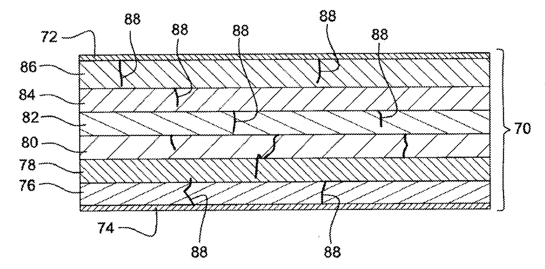
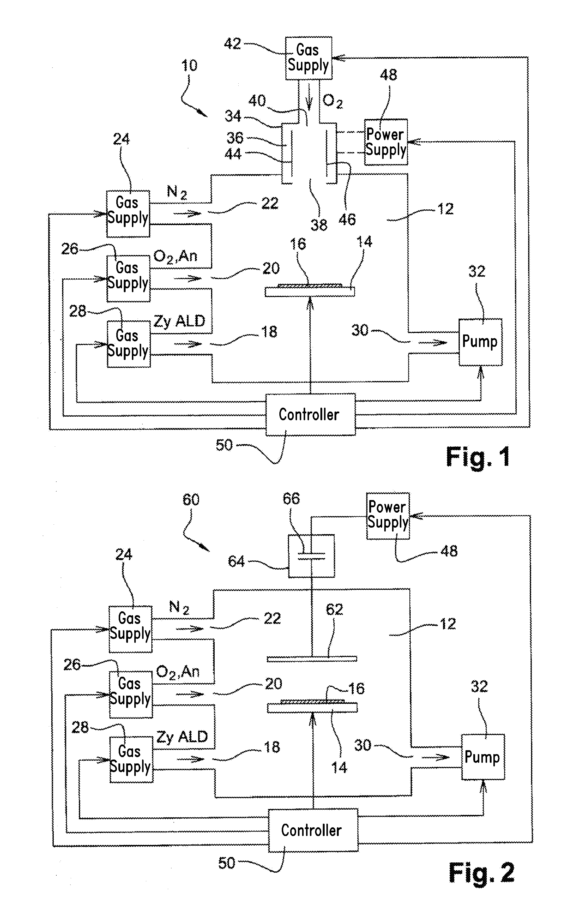
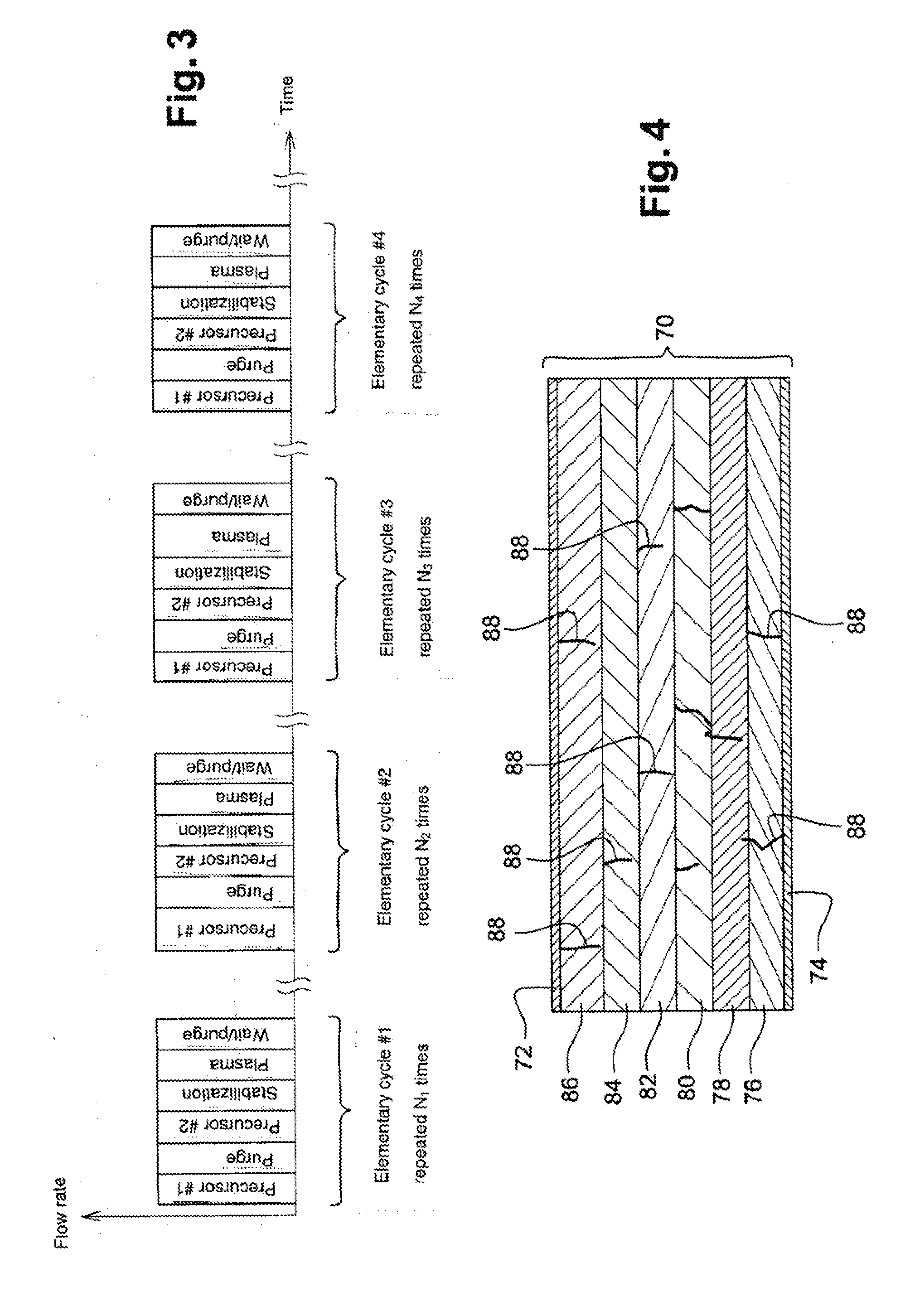
[0030]FIG. 1 shows a first example of a PEALD system 10 for manufacturing a polycrystalline dielectric layer, such as a polycrystalline dielectric oxide layer, on a metal substrate 16—a capacitor electrode for example, and more particularly a polycrystalline layer made of a single dielectric oxide and having a crystallization rate greater than 70 percent, and preferably greater that 80 percent.

[0031]System 10 comprises a hermetically sealed reaction vessel 12 in which a plate 14 is placed in order to accommodate metal substrate 16. Plate 14 comprises controllable means of adjusting its temperature (not shown) such as a heating resistance. Other means of heating can be envisaged such as heating by lamps for example.

[0032]Reaction vessel 12 has a first inlet opening 18 for feeding in a first precursor of the dielectric oxide that is to be deposited, a second inlet opening 20 for feeding in a second precursor of the dielectric oxide that is to be deposited and a third inlet opening 22 ...


PUM

PropertyMeasurementUnit
Fractionaaaaaaaaaa
Thicknessaaaaaaaaaa
Dielectric polarization enthalpyaaaaaaaaaa

Abstract

A method manufactures a capacitor having polycrystalline dielectric layer between two metallic electrodes. The dielectric layer is formed by a polycrystalline growth of a dielectric metallic oxide on one of the metallic electrodes. At least one polycrystalline growth condition of the dielectric oxide is modified during the formation of the polycrystalline dielectric layer, which results in a variation of the polycrystalline properties of the dielectric oxide within the thickness of said layer.

Description

BACKGROUND[0001]1. Technical Field[0002]The disclosure relates to the field of manufacturing a polycrystalline dielectric layer on metal and, more especially, manufacturing a dielectric capacitor layer inserted between two metal electrodes.[0003]2. Description of the Related Art[0004]Dielectric layers that have a high dielectric constant have many applications, especially in compact, high-capacitance capacitors.[0005]The dielectric constant of a dielectric material depends not only on the atoms of which it is made but also on the spatial arrangement of the molecules relative to each other. For example, zirconium oxide (ZrO2) has a dielectric constant equal to 18 in its amorphous form, i.e. a form that has no particular structure, and a dielectric constant of 45 when it has a tetragonal or cubic crystalline structure.[0006]One way of increasing the capacitance of a capacitor without increasing the volume of its dielectric layer is therefore to produce the latter in a crystalline form...

Claims


Application Information

Patent Timeline
IPC IPC(8): H01G4/20C23C16/50B05D5/12
CPCH01G4/33Y10T29/43H01L21/0228Y10T29/435H01G4/1209H01L21/02189C23C16/45542H01G4/085C23C16/45529C23C16/405H01L21/02274H01L28/40Y10T29/42
Inventor GROS-JEAN, MICKAEL
Owner STMICROELECTRONICS (CROLLES 2) SAS
Why Eureka
Try Eureka