Substrate assembly provided with capacitive interconnections, and manufacturing method thereof
- Summary
- Abstract
- Description
- Claims
- Application Information
AI Technical Summary
Benefits of technology
Problems solved by technology
Method used
Image
Examples
Embodiment Construction
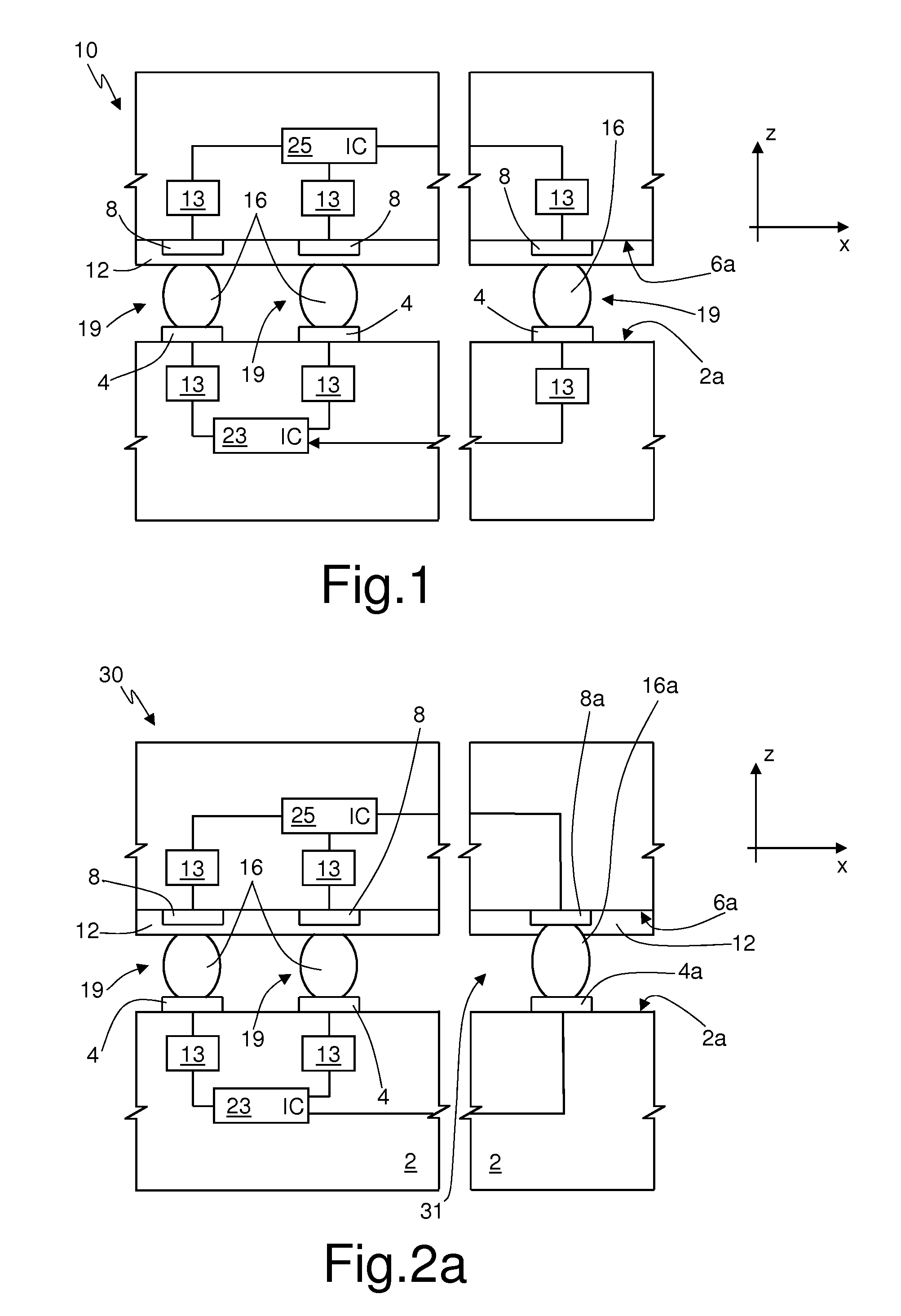
[0047]FIG. 1 shows, in cross-sectional view, an assembly of two substrates according to an embodiment, forming, for example, an electronic device 10.
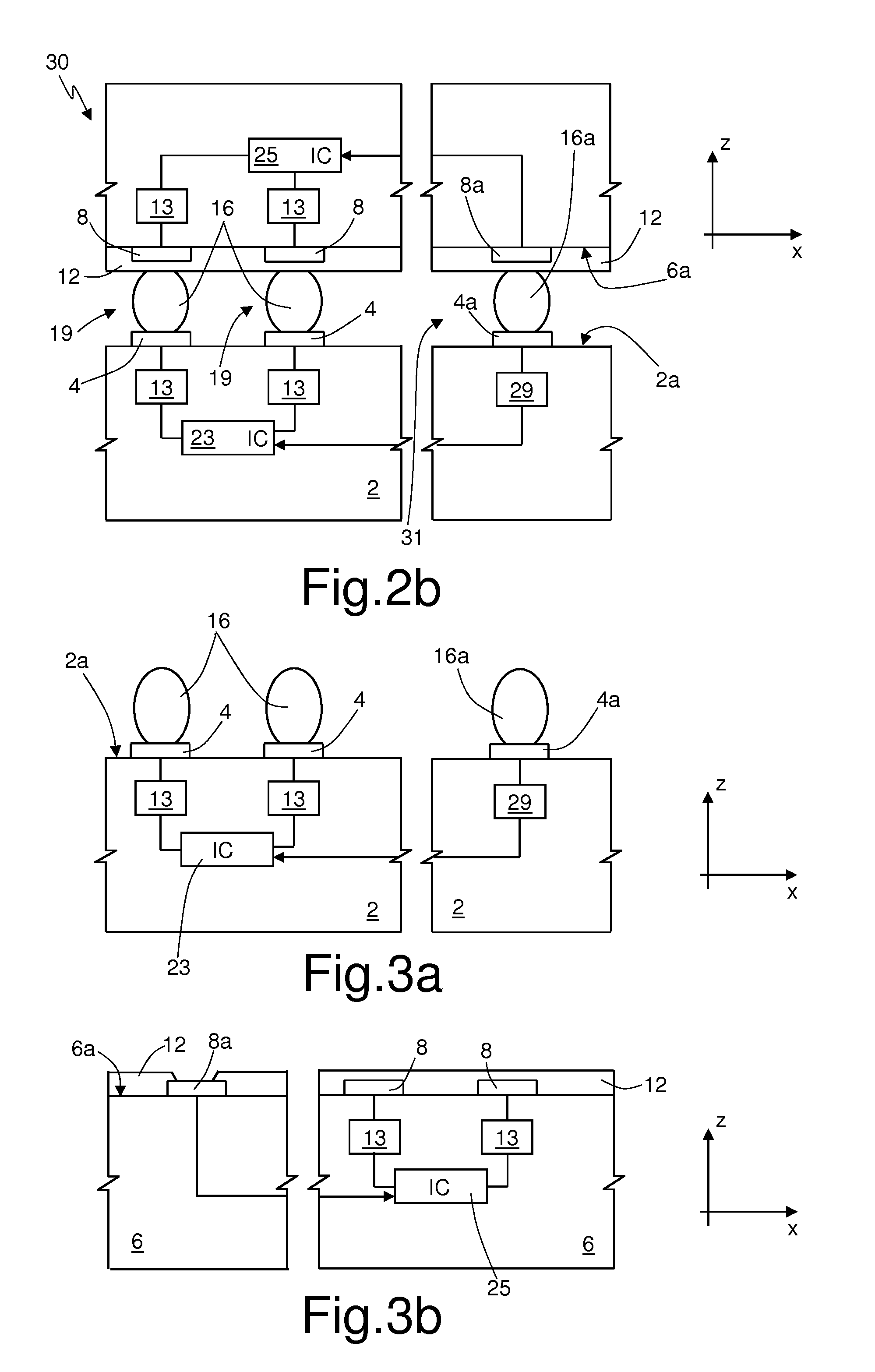
[0048]In detail, the electronic device 10 comprises a first substrate 2 and a second substrate 6, for example made of semiconductor material, such as silicon.
[0049]The first substrate 2 is provided with first conductive pads 4, formed on a surface 2a of the first substrate 2, and the second substrate 6 is provided with second conductive pads 8 formed on a surface 6a of the second substrate 6. FIG. 1 shows, by way of example, three first conductive pads 4 and three second conductive pads 8. It is evident that, according to the need, the first and second conductive pads 4, 8 can be in any number, higher or lower than three.
[0050]The second substrate 6 moreover includes a dielectric layer 12, formed on top of the surface 6a and on top of the second conductive pads 8. The dielectric layer 12 is, according to an embodiment, a passivation lay...
PUM
| Property | Measurement | Unit |
|---|---|---|
| Temperature | aaaaa | aaaaa |
| Electrical conductor | aaaaa | aaaaa |
| Melting point | aaaaa | aaaaa |
Abstract
Description
Claims
Application Information
 - R&D Engineer
- R&D Manager
- IP Professional
- Industry Leading Data Capabilities
- Powerful AI technology
- Patent DNA Extraction
Browse by: Latest US Patents, China's latest patents, Technical Efficacy Thesaurus, Application Domain, Technology Topic, Popular Technical Reports.
© 2024 PatSnap. All rights reserved.Legal|Privacy policy|Modern Slavery Act Transparency Statement|Sitemap|About US| Contact US: help@patsnap.com


