Substrate processing apparatus

a processing apparatus and substrate technology, applied in the direction of electrical apparatus, electric discharge tubes, basic electric elements, etc., can solve the problem of difficult to remove the deposits attached to the inner focus ring by using an ashing process

Active Publication Date: 2012-07-12
TOKYO ELECTRON LTD
View PDF4 Cites 35 Cited by
  • Summary
  • Abstract
  • Description
  • Claims
  • Application Information

AI Technical Summary

Benefits of technology

[0012]The present invention provides a substrate processing apparatus capable of removing deposits attached on a component having a lower temperature in a gap between two components having a large temperature difference, without degrading a working ratio of the substrate processing apparatus.

Problems solved by technology

Since the gap between the inner focus ring and the outer focus ring is narrow and it is difficult for plasma to enter the gap, it is difficult to remove deposits attached onto the inner focus ring by using an ashing process or the like.

Method used


Image

  • Substrate processing apparatus
  • Substrate processing apparatus
  • Substrate processing apparatus

Examples


first embodiment

[0034]First, a substrate processing apparatus according to the present invention will be described.

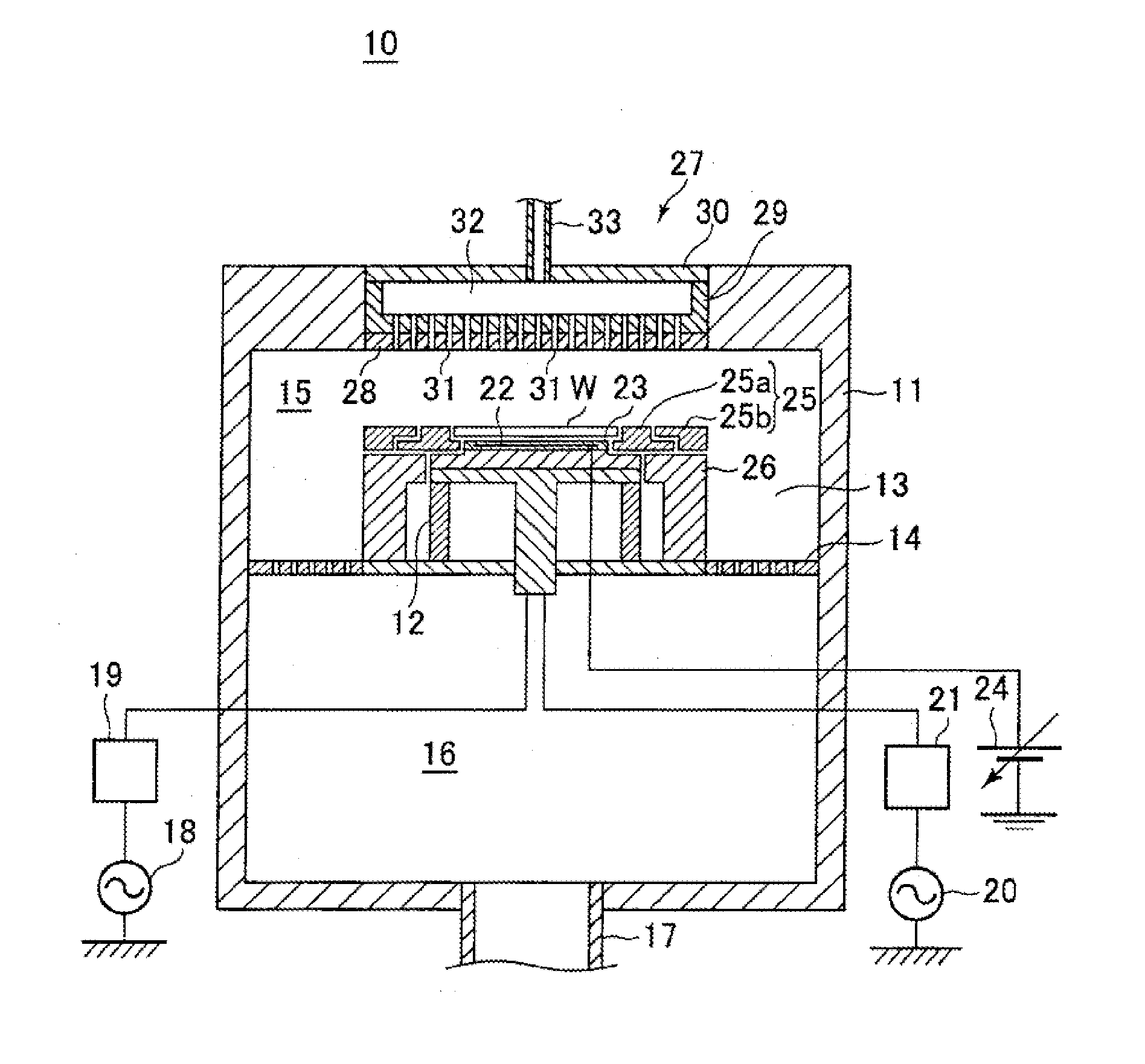
[0035]FIG. 1 is a diagram schematically showing a configuration of a substrate processing apparatus 10 according to the present embodiment. The substrate processing apparatus 10 of the present embodiment performs a plasma etching process on a wafer for forming semiconductor devices (hereinafter, simply referred to as ‘wafer’) as a substrate.

[0036]Referring to FIG. 1, the substrate processing apparatus 10 includes a chamber 11 for receiving a wafer W having a diameter of, for example, 300 mm, and a susceptor 12 (holding stage) formed as a cylinder on which the wafer W is placed is disposed in the chamber 11. In the substrate processing apparatus 10, a side exhaust passage 13 is formed by an inner side wall of the chamber 11 and a side surface of the susceptor 12. An exhaust plate 14 is disposed at an intermediate portion of the side exhaust passage 13.

[0037]The exhaust plate 14 is forme...

second embodiment

[0055]Next, a substrate processing apparatus according to the present invention will be described.

[0056]The substrate processing apparatus according to the present embodiment basically has the same structures and the same operations as those of the substrate processing apparatus according to the first embodiment, and thus descriptions about the same structures and the same operations are not provided here, and different configurations and operations from those of the previous embodiment will be described as follows.

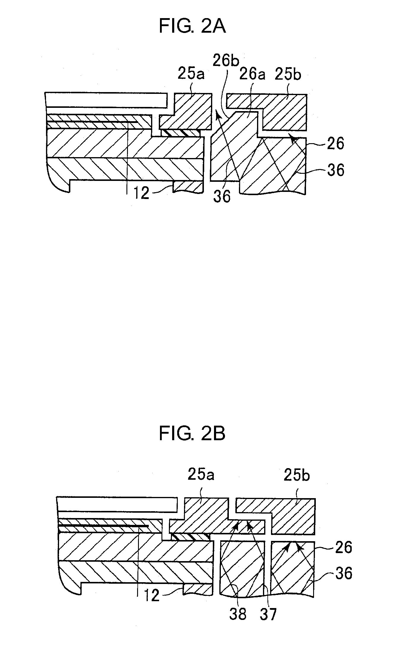
[0057]FIGS. 3A and 3B are magnified cross-sectional views schematically showing a structure around a focus ring included in the substrate processing apparatus 10 according to the present embodiment, wherein FIG. 3A shows the substrate processing apparatus 10 according to the present embodiment and FIG. 3B shows a modified example of the substrate processing apparatus 10 according to the present embodiment.

[0058]Referring to FIG. 3A, the substrate processing apparatus 10 f...

third embodiment

[0061]Next, a substrate processing apparatus according to the present invention will be described.

[0062]The substrate processing apparatus according to the present embodiment basically has the same structures and the same operations as those of the substrate processing apparatus according to the first embodiment, and thus descriptions about the same structures and the same operations are not provided here, different configurations and operations from those of the first embodiment will be described as follows.

[0063]In the substrate processing apparatus 10 shown in FIG. 1, a gap of a predetermined width is formed between the side surface of the susceptor 12 and an inner side surface of the inner focus ring 25a in order to easily attach / detach the focus ring 25 to / from the susceptor 12. However, the susceptor 12 is directly cooled down by the cooling unit built therein, and accordingly, a temperature of susceptor 12 is much lower than the temperature of the inner focus ring 25a. That i...


PUM

PropertyMeasurementUnit
wavelengthaaaaaaaaaa
diameteraaaaaaaaaa
pressureaaaaaaaaaa

Abstract

A substrate processing apparatus capable of removing deposits attached on a component of a lower temperature in a gap between two components, temperatures of which are greatly different from each other, without degrading a working ratio of the substrate processing apparatus. In the substrate processing apparatus, a chamber receives a wafer, a focus ring surrounds the wafer disposed in the chamber, a side surface protective member transmits a laser beam, a laser beam irradiating apparatus irradiates the laser beam to the side surface protective member, an inner focus ring of the focus ring is disposed adjacent to the wafer and is cooled down and an outer focus ring surrounds the inner focus ring and is not cooled down in a focus ring, and a facing surface of the side surface protective member faces a gap between the inner focus ring and the outer focus ring.

Description

CROSS-REFERENCE TO RELATED PATENT APPLICATIONS[0001]This application claims the benefit of Japanese Patent Application No. 2011-002251 filed on Jan. 7, 2011, in the Japan Patent Office and U.S. Patent Application Ser. No. 61 / 435,094, filed on Jan. 21, 2011, in the United States Patent and trademark Office, the disclosure of which are incorporated herein in their entireties by reference.BACKGROUND OF THE INVENTION[0002]1. Field of the Invention[0003]The present invention relates to a substrate processing apparatus including a focus ring.[0004]2. Description of the Related Art[0005]Recently, semiconductor wafers (hereinafter, simply referred to as ‘wafers’) from which semiconductor devices are fabricated have been enlarged, and accordingly, it is required that semiconductor devices be obtained from peripheral portions of wafers, for example, a range within 10 mm toward centers of wafers from peripheries of the wafers. However, since distribution of radicals in plasma used to process a...

Claims


Application Information

Patent Timeline
Patent Type & Authority Applications(United States)
IPC IPC(8): H01L21/3065
CPCH01J37/32477H01J37/32559H01L21/68735H01L21/67069H01J37/32642
Inventor YAMAWAKU, JUNKOSHIMIZU, CHISHIO
Owner TOKYO ELECTRON LTD
Why Eureka
Try Eureka