Power semiconductor package structure and manufacturing method thereof

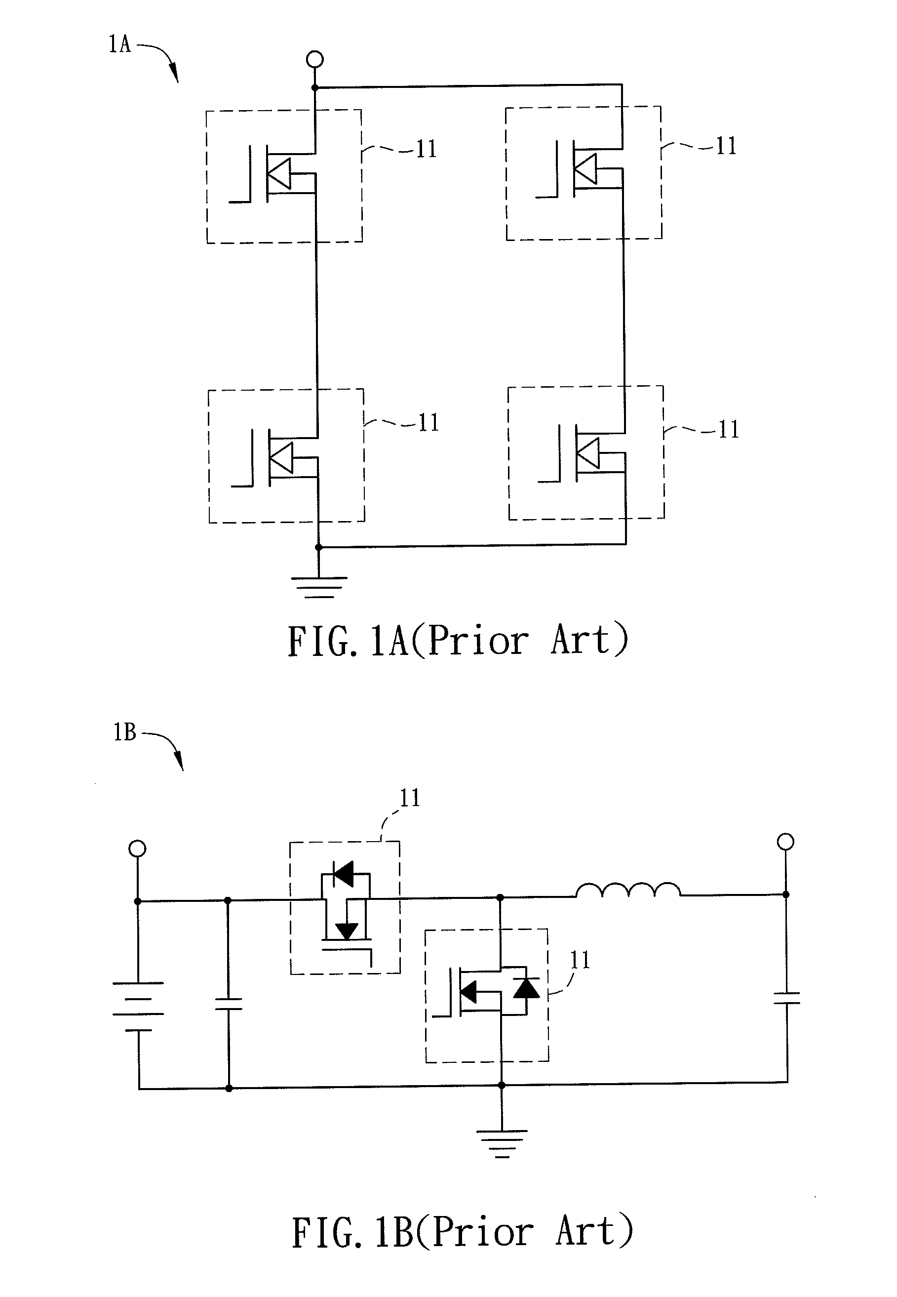
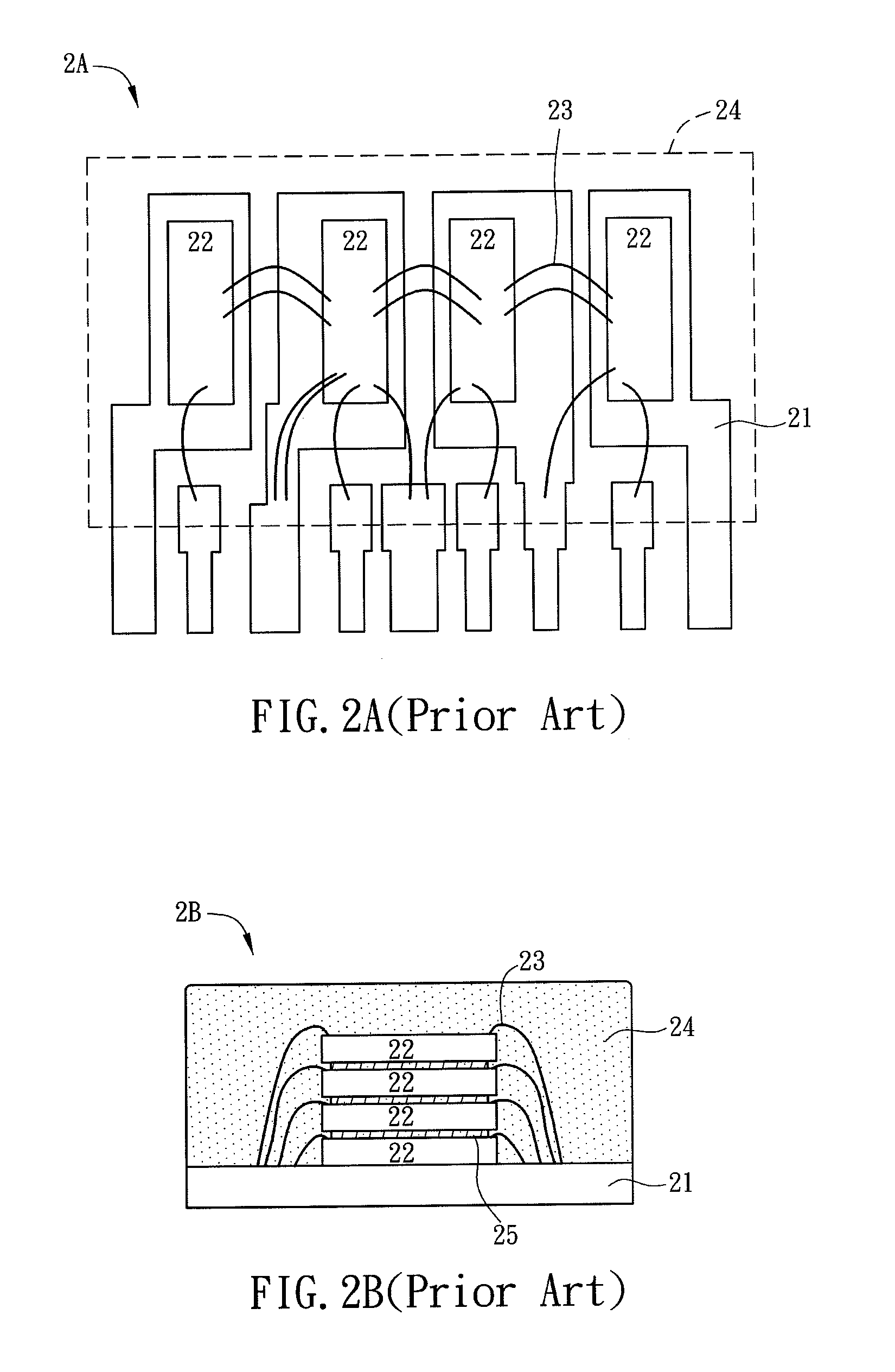
a technology of power semiconductor and package structure, applied in the direction of semiconductor devices, semiconductor/solid-state device details, electrical apparatus, etc., can solve the problems of poor space use, over-the-counter surface integration and wire bonding technology still has many drawbacks, and the contact surface between the wire and the source cannot cover the most area of the source, so as to improve efficiency and reduce parasitic effect , the effect of increasing reliability

Active Publication Date: 2012-07-19
DELTA ELECTRONICS INC
View PDF23 Cites 20 Cited by
  • Summary
  • Abstract
  • Description
  • Claims
  • Application Information

AI Technical Summary

Benefits of technology

[0035]As mentioned above, in the power semiconductor package structure of the present invention, at least a part of the first control electrode, which is disposed underneath the first power chip, is non-covered by the second power chip stacked thereabove along a projection direction perpendicular to the carrier. Thus, it is unnecessary to apply additional protection material to isolate the first control electrode from the bottom of the second power chip. In addition, the present invention uses the conductive sheets to electrically connect the electrodes of the first and second power chips, so that the parasitic effect caused by the bonding wires can be avoided. Accordingly, the reliability can be increased, the parasitic effect can be reduced, and the efficiency can be enhanced.

Problems solved by technology

However, this connection has the issues of poor usage in space and obvious parasitic effect.
However, the above technologies of surface integration and wire bonding still have many drawbacks.
In addition, due to the limitation of the wire bonding process, the contact surface between the wire and the source can not cover most area of the source (usually less than 70%).
Moreover, since the lateral resistance of the chip is larger, the current distribution between the source and drain of the chip is non-uniform, which is different from the ideal situation, and the current may be concentrated at some points.
Besides, the resistance of the wire is usually larger, so the current parasitic effect is very obvious.
In addition, the gaps between the electrodes of the chips 22 must be completely covered by the molding compound 24 so as to achieve the desired isolation and prevent the undesired bubbles, which may decrease the reliability of the package.
This may make the flowing / filling of the molding compound 24 more difficult so as to form some pores or bubbles, thereby decreasing the reliability of the package structure.
These additional auxiliary processes may increase the complex of the manufacturing processes.
Accordingly, the ripple of the component is increased, or the switching speed of the component is affected, which dramatically increases the on loss and switching loss.

Method used


Image

  • Power semiconductor package structure and manufacturing method thereof
  • Power semiconductor package structure and manufacturing method thereof
  • Power semiconductor package structure and manufacturing method thereof

Examples


Embodiment Construction

[0053]The present invention will be apparent from the following detailed description, which proceeds with reference to the accompanying drawings, wherein the same references relate to the same elements.

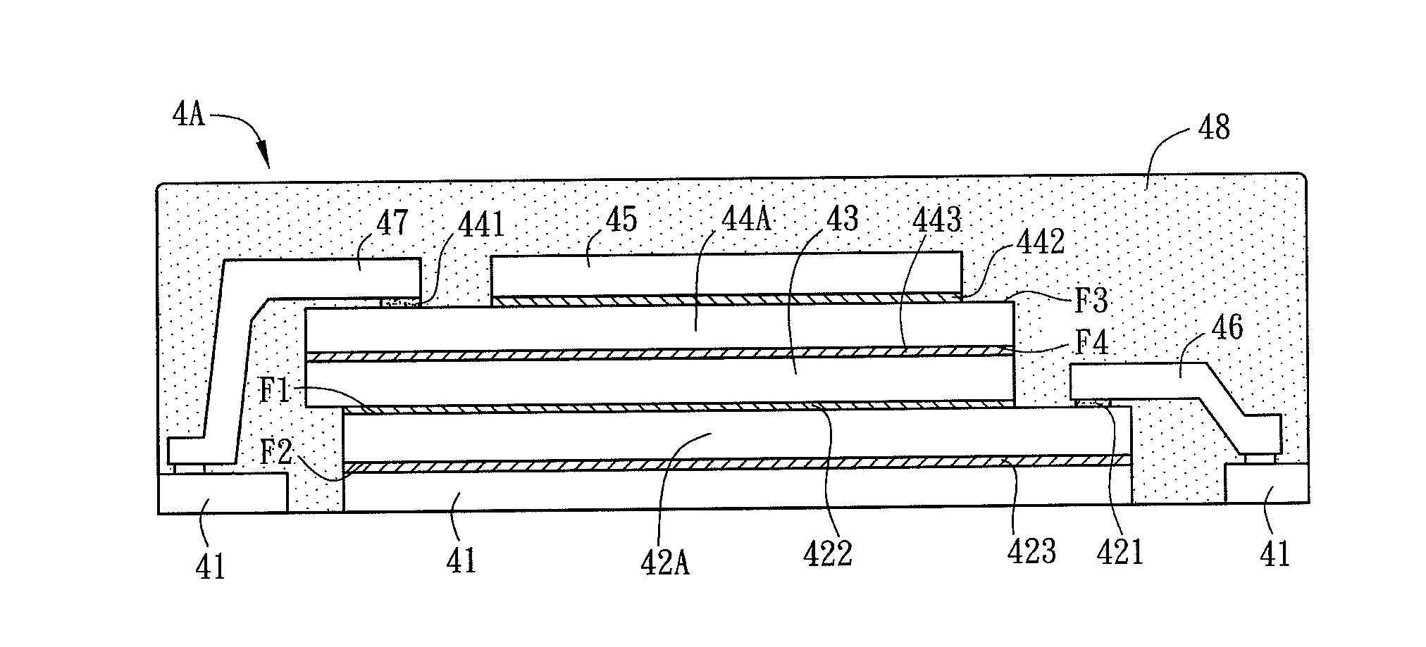
[0054]FIG. 3 is a perspective view of a power semiconductor package structure 3 according to a preferred embodiment of the present invention. As shown in FIG. 3, the power semiconductor package structure 3 includes a carrier 31, a first power chip 32, a first conductive sheet 33, a second power chip 34, a second conductive sheet 35, and a third conductive sheet 36.

[0055]The first power chip 32 has a first surface, a second surface, a first control electrode (not shown), a first main power electrode (not shown), and a second main power electrode (not shown). The first and second surfaces are disposed opposite to each other, and the second surface is connected to the carrier 31. The first control electrode and the first main power electrode are disposed on the first surface, and the sec...


PUM


Abstract

A power semiconductor package structure includes a carrier, a first power chip, a second power chip, a first conductive sheet, a second conductive sheet and a third conductive sheet. The first power chip has a first surface and a second surface opposing to the first surface. A first control electrode and a first main power electrode are disposed on the first surface, and a second main power electrode is disposed on the second surface. The second surface is disposed on the carrier, and electrically connected to the carrier through the second main power electrode. The second power chip has a third surface and a fourth surface opposing to the third surface. A third main power electrode is disposed on the third surface, and a fourth main power electrode is disposed on the fourth surface. The fourth surface is disposed on the first power chip. The first conductive sheet is electrically connected to the first main power electrode and the fourth main power electrode. The second conductive sheet is electrically connected to the third main power electrode. The third conductive sheet is electrically connected to the first control electrode. At least a part of the first control electrode is non-covered by the second power chip along a projection direction, which is perpendicular to the carrier.

Description

CROSS REFERENCE TO RELATED APPLICATIONS[0001]This Non-provisional application claims priority under 35 U.S.C. §119(a) on Patent Application No(s). 201110020133.1 filed in People's Republic of China on Jan. 18, 2011, the entire contents of which are hereby incorporated by reference.BACKGROUND OF THE INVENTION[0002]1. Field of Invention[0003]The present invention relates to a package structure and a manufacturing method thereof. In particular, the present invention relates to a power semiconductor package structure and a manufacturing method thereof.[0004]2. Related Art[0005]Higher efficiency and higher density are always the demands for the power converters. The higher efficiency indicates the lower power loss, so that this feature can help the power saving. The higher density indicates the smaller product size, so that this feature can achieve the product design of compact and light.[0006]FIG. 1A shows a full-bridge circuit 1A used in the conventional power converter, and FIG. 1B sh...

Claims


Application Information

Patent Timeline
Patent Type & Authority Applications(United States)
IPC IPC(8): H01L23/538H01L21/50
CPCH01L2924/1306H01L2224/48247H01L23/49524H01L23/49562H01L23/49575H01L25/071H01L25/074H01L2224/291H01L2224/2919H01L2224/32155H01L2224/32225H01L2224/32245H01L2224/48227H01L2224/73215H01L2224/73265H01L2924/1203H01L2924/13055H01L2924/13091H01L2924/19041H01L2924/19103H01L2924/1305H01L2924/3011H01L2224/49111H01L2224/48137H01L23/3107H01L2224/32145H01L2224/48091H01L2924/00H01L2924/00012H01L2924/00014H01L24/73H01L2924/181H01L2224/40245H01L2224/2612H01L2224/73221
Inventor ZENG, JIAN-HONGHONG, SHOU-YU
Owner DELTA ELECTRONICS INC
Why Eureka
Try Eureka