Supercharge Your Innovation With Domain-Expert AI Agents!

ESD protection structure

a protection circuit and electrostatic discharge technology, applied in emergency protection arrangements, diodes, electrical equipment, etc., can solve the problems of low production yield, achieve the effect of enhancing esd protection ability, reducing the area of esd protection circuits, and increasing production yield

Inactive Publication Date: 2012-07-19
BEYOND INNOVATION TECH
View PDF5 Cites 7 Cited by
  • Summary
  • Abstract
  • Description
  • Claims
  • Application Information

AI Technical Summary

Benefits of technology

[0008]Accordingly, the invention is directed to an ESD protection structure capable of enhancing the ESD protection ability, reducing the area of an ESD protection circuit and even increasing the production yield.
[0011]Based on the mentioned above, a parasitic diode (i.e., the ESD protection component) is formed at a PN junction between the first doped region and the body. The present invention utilizes the space under the bonding pad and disposes the first doped region electrically connected to the bonding pad so that the area of the ESD protection circuit is reduced. Since the electrical path distance between the bonding pad and the ESD protection component is largely reduced, the ESD protection ability can be advanced. Moreover, even though the bonding pad contacts the first doped region of the IC substrate when the vertical stress is too large during wire bonding, the function of the IC still is not affected and the production yield can be increased.

Problems solved by technology

Sometimes, when the vertical stress during wire bounding is too large, the stress even makes the bonding pad 111 electrically contact the IC substrate 210 and leads to a low production yield.

Method used


Image

  • ESD protection structure
  • ESD protection structure
  • ESD protection structure

Examples


Embodiment Construction

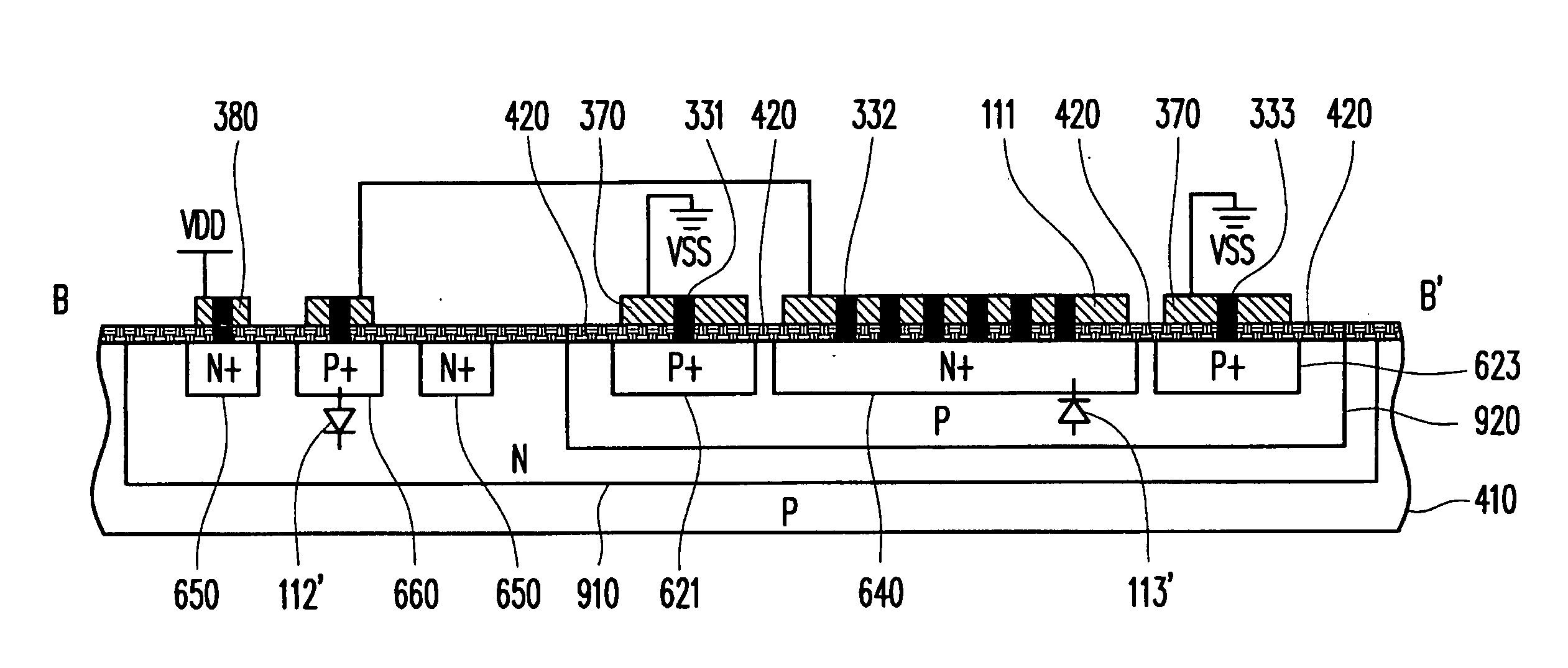
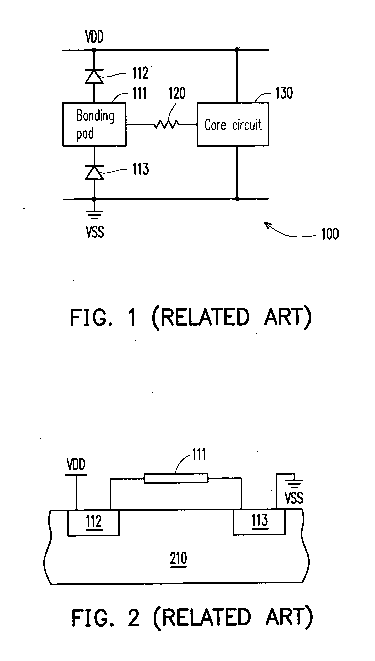
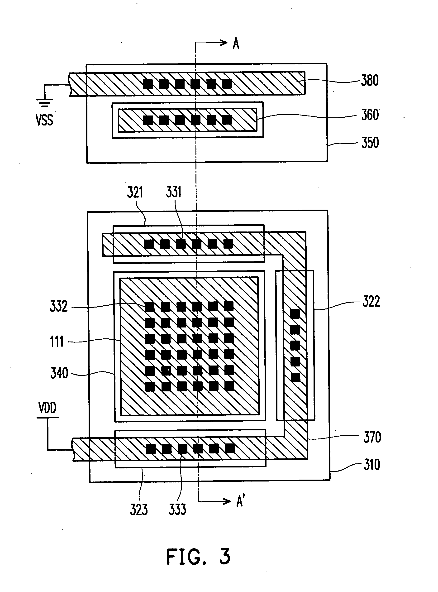
[0023]FIG. 3 is a top view diagram of a layout structure equivalent to that of the ESD protection components 112 and 113 and the bonding pad 111 in FIG. 1 in the prior art according to an embodiment of the invention. FIG. 4 is a cross-sectional diagram of the ESD protection structure in FIG. 3 along A-A′ line according to another embodiment of the invention. Referring to FIGS. 3 and 4, a body (or buck) 310 is a first conductive type, wherein the first conductive type is assumed to be N-doped conductive type, and the body 310 is an N-well disposed in an IC substrate 410. The IC substrate 410 is a second conductive type, wherein the second conductive type is assumed to be P-doped conductive type.

[0024]A first doped region 340 herein is a P-type heavy doped region (P+ area). The first doped region 340 is disposed in the body 310 so that a parasitic diode 112′ is formed at the PN junction between the first doped region 340 and the body 310, and the parasitic diode 112′ can be equivalent...


PUM


Abstract

An electrostatic discharge (ESD) protection structure is provided, which includes a bonding pad, a body, an insulation layer, a first doped region and a via. The body is a first conductive type, while the first doped region is a second conductive type. The bonding pad is disposed on the body. The insulation layer is disposed between the body and the bonding pad. The first doped region is disposed in the body, and in view direction along the vertical projection of the body, all of the bonding pad is disposed in the first doped region. The via is disposed between the first doped region and the bonding pad. The bonding pad is electrically connected to the first doped region through the via.

Description

CROSS-REFERENCE TO RELATED APPLICATION[0001]This application claims the priority benefit of Taiwan application serial no. 99127789, filed Aug. 19, 2010. The entirety of the above-mentioned patent application is hereby incorporated by reference herein and made a part of this specification.BACKGROUND OF THE INVENTION[0002]1. Field of the Invention[0003]The invention generally relates to a layout structure of an integrated circuit (IC), and more particularly, to a layout structure of an electrostatic discharge (ESD) protection circuit under a bonding pad.[0004]2. Description of Related Art[0005]In a real application environment, ESD come from various sources would shock an electronic product. When ESD occurs, the sudden ESD current may burn a component instantaneously. In order to overcome the above-mentioned problem, usually some ESD mechanisms are designed and placed in the circuit so as to effectively guide the ESD current out to avoid the component from being burned.[0006]FIG. 1 is...

Claims


Application Information

Patent Timeline
Patent Type & Authority Applications(United States)
IPC IPC(8): H02H9/04
CPCH01L27/0255
Inventor JUNG, KUANG-YU
Owner BEYOND INNOVATION TECH
Features
  • R&D
  • Intellectual Property
  • Life Sciences
  • Materials
  • Tech Scout
  • Unparalleled Data Quality
  • Higher Quality Content
  • 60% Fewer Hallucinations
Learn More