Fractal interconnects for neuro-electronic interfaces and implants using same

a neuro-electronic interface and fractal technology, applied in the field of artificial electronic implants, can solve the problems of electrical signals from the electrodes affecting the plexiform layer, not solving other problems with the design, and many potential problems

Active Publication Date: 2012-08-16
CANTERGURY UNIV OF +1
View PDF1 Cites 23 Cited by
  • Summary
  • Abstract
  • Description
  • Claims
  • Application Information

AI Technical Summary

Benefits of technology

[0011]In another aspect, a method is provided for fabricating a neuro-electronic interconnect. The method includes providing a micro-electrode array comprising a collection of electrodes and a non-conductive planar layer forming an interspace between the electrodes, forming nanoscale particles, and depositing the nanoscale particles onto the planar layer to produce conductive interconnects in electrical contact with the electrodes. The depositing of the nanoscale particles includes controlling a diffusivity of the clusters such that each of the produced interconnects has scaling gradients that can range between 1.1 and 1.9 over a scaling range of at least one order of magnitude. In some cases, the interconnect has a fractal dimension D between 1.4 and 1.9 over a scaling range of at least one order of magnitude below 200 μm. In some cases, the diffusivity is controlled such that each of the produced interconnects has a fractal dimension D between 1.6 and 1.9 over a scaling range of at least two orders of magnitude below 200 μm. Implementations of the method may include forming the nanoscale particles by a) inert gas aggregation, b) atomic cluster evaporation (from a crucible). In some embodiments of the method, the micro-electrode array comprises a substrate, the electrodes are fabricated on the substrate, and the method includes depositing the planar layer onto the substrate of the micro-electrode array such that the planar layer covers the planar substrate but does not completely cover the electrodes, and a surface roughness of the planar layer is less than a surface roughness of the substrate. In some cases depositing the planar layer is performed such that the deposited planar layer has a mean roughness (Rms) less than 1 nm.

Problems solved by technology

The design shown in FIG. 2A, however, has several potential problems.
One significant problem is that electrical signals from the electrodes may damage the plexiform layer due to a capacitance overload at the interface or induce toxins due to polarization of electrolytic bio-fluid at the interface.
This approach, however, does not solve other problems with the design.
Another potential problem is that many electrodes in the array may be unconnected or poorly connected to neurons in the plexiform layer.
Although photodiodes can be fabricated with packing densities approaching those of the rods and cones in the human retina, a person with an artificial retina might still only be able to see a small fraction of the detail generated by the implant.
Although increasing the size of each electrode 202 might be expected to improve the likelihood that it will connect with a neuron, this approach is not feasible for a retinal implant since it would obscure light from reaching the underlying photodiode 200 and defeat the fundamental purpose of the implant.
Moreover, electronic implants in other parts of the body also suffer from similar challenges related to insufficient number of neuro-electrical connections.
Prosthetic hands, for example, do not have an adequate connection with the nerves to provide an adequate sense of touch.
Similarly, the number of connections between neurons and electrodes implanted into mammalian brains is insufficiently large to accurately target neurons requiring electrical stimulation.
The same problem is faced by implants designed to interface two parts of a biological system that have lost their natural connection.
In each case, the functionality of the implant is limited by the performance of the neuro-electrical interface between the artificial and biological systems.

Method used


Image

  • Fractal interconnects for neuro-electronic interfaces and implants using same
  • Fractal interconnects for neuro-electronic interfaces and implants using same
  • Fractal interconnects for neuro-electronic interfaces and implants using same

Examples


Embodiment Construction

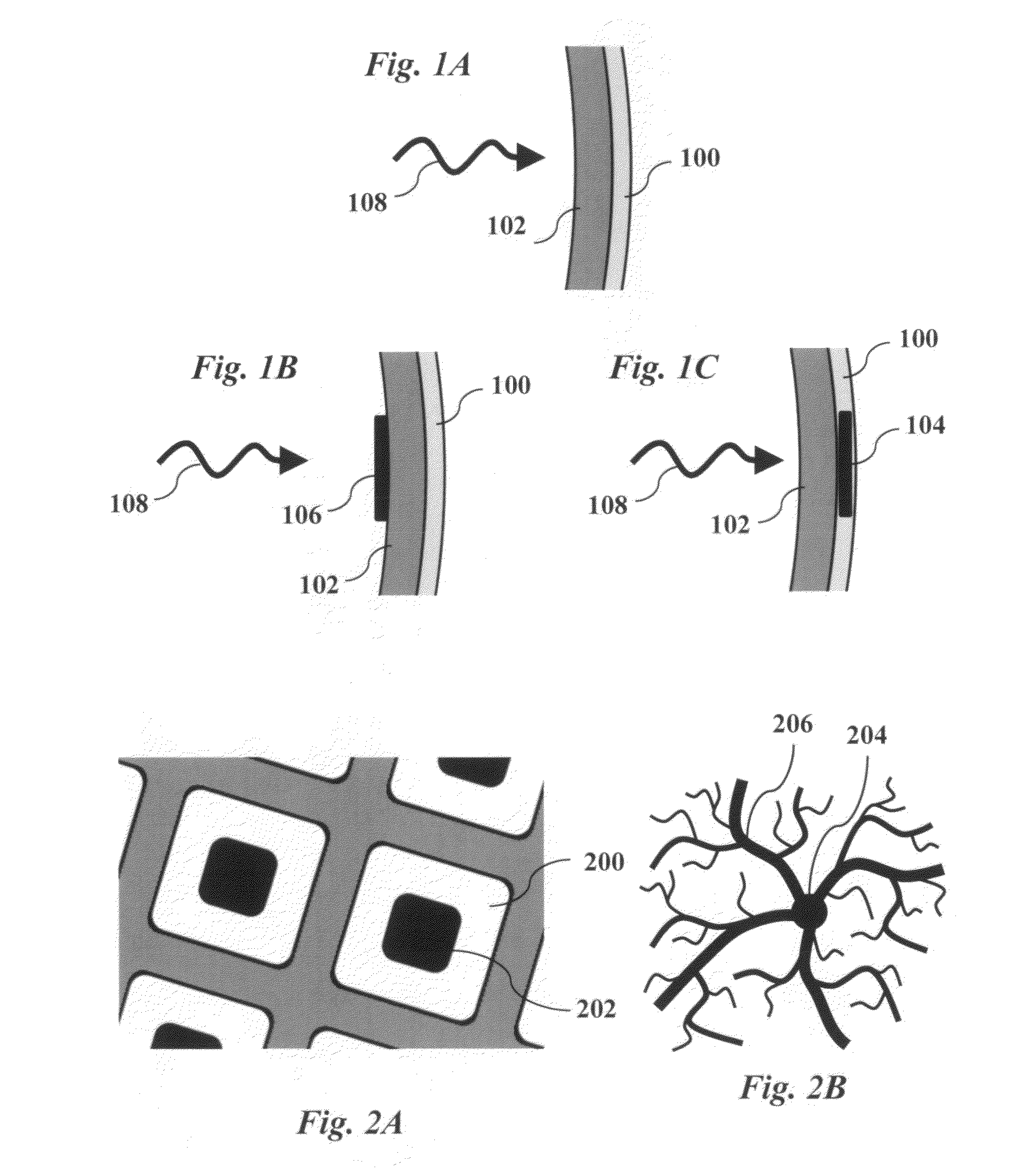
[0037]Embodiments of the present invention include a method for fabricating fractal interconnects to improve the neuro-electronic interface between biological organisms and artificial electronic implants such as artificial retinal implants, artificial brain implants and artificially-generated neuron systems. Embodiments also include neuro-electronic interconnect devices and the implant devices incorporating them. Such fractal interconnect devices provide a neuro-electronic interface between the electrodes of an implant and the neurons of a human or animal. The principles of the present invention have general application to many types of electronic implants and other devices that rely upon neuro-electrical interfaces.

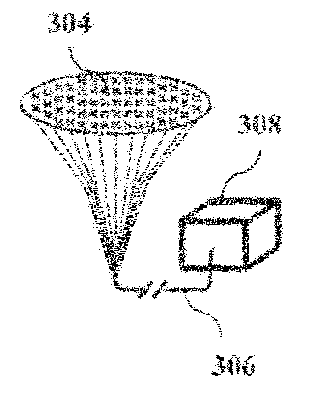
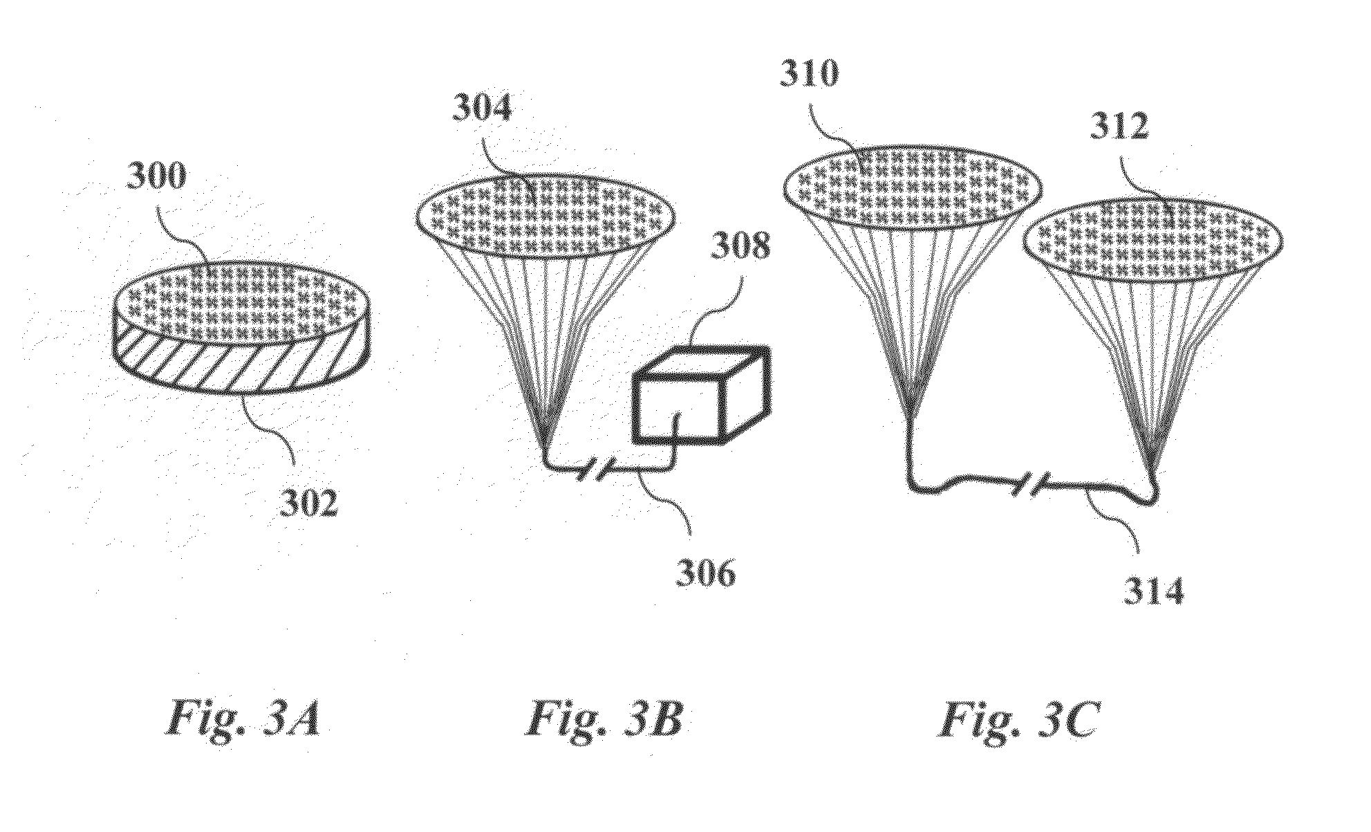
[0038]FIG. 3A is a schematic diagram showing one embodiment of the invention in the form of an implant having an array of fractal interconnects 300 integrated with an electronic chip 302. For example, this type of device may be a retinal implant in the form of a 3 mm sub...


PUM


Abstract

A neuro-electronic interface device has a micro-electrode electrically connected to an interconnect that has scaling gradients between 1.1 and 1.9 over a scaling range of at least one order of magnitude. The device preferably has an array of such fractal interconnects in electrical contact with an array of micro-electrodes. Such fractal interconnect arrays may be components of implants including a retinal implant device having an array of photodetectors in electrical contact with the array of micro-electrodes. The interconnects may be fabricated by forming nanoscale particles and depositing them onto a non-conductive surface that is smooth except for electrodes which serve as nucleation sites for the formation of fractal interconnect structures through diffusion limited aggregation.

Description

FIELD OF THE INVENTION[0001]The present invention relates generally to artificial electronic implants for humans and animals. More specifically, it relates to techniques and devices for neuro-electronic interface devices used to form a connection between an electronic implant and biological neurons.BACKGROUND OF THE INVENTION[0002]Electronic implants can dramatically improve the quality of human life. Due to the development of nanoelectronics, there is now the possibility of integrating implants with more sophisticated physiological systems such as the visual system.[0003]The visual system includes the retina, which receives light and converts it into electrical signals; the optic nerve, which communicates the signals from the retina to the brain; and the visual regions of the brain, which process the signals. Diseases such as macular degeneration deteriorate the retina while leaving the optic nerve healthy. Accordingly, to restore vision, researchers have proposed artificial retina...

Claims


Application Information

Patent Timeline
Patent Type & Authority Applications(United States)
IPC IPC(8): A61F9/08A61N1/04
CPCA61N1/0526B82Y30/00A61N1/36103A61N1/0543
Inventor TAYLOR, RICHARD P.BROWN, SIMON A.
Owner CANTERGURY UNIV OF
Why Eureka
Try Eureka