Lighting device and method for manufacturing the same

a technology of light-emitting devices and manufacturing methods, which is applied in the direction of lenses, instruments, optical elements, etc., can solve the problems that the efficiency of extracting light from the inside of the light-emitting element to the air cannot reach 100%, and achieve the effect of high efficiency and reduced manufacturing costs of the lighting devi

Inactive Publication Date: 2012-08-30
SEMICON ENERGY LAB CO LTD
View PDF6 Cites 73 Cited by
  • Summary
  • Abstract
  • Description
  • Claims
  • Application Information

AI Technical Summary

Benefits of technology

[0010]Further, an object of one embodiment of the disclosed invention is to suppress the manufacturing cost of the lighting device.
[0044]According to one embodiment of the disclosed invention, the manufacturing cost of the lighting device can be reduced.

Problems solved by technology

As a result, efficiency in extracting light from the inside of the light-emitting element to the air does not reach 100%.

Method used


Image

  • Lighting device and method for manufacturing the same
  • Lighting device and method for manufacturing the same
  • Lighting device and method for manufacturing the same

Examples


embodiment 1

Structure of Lighting Device

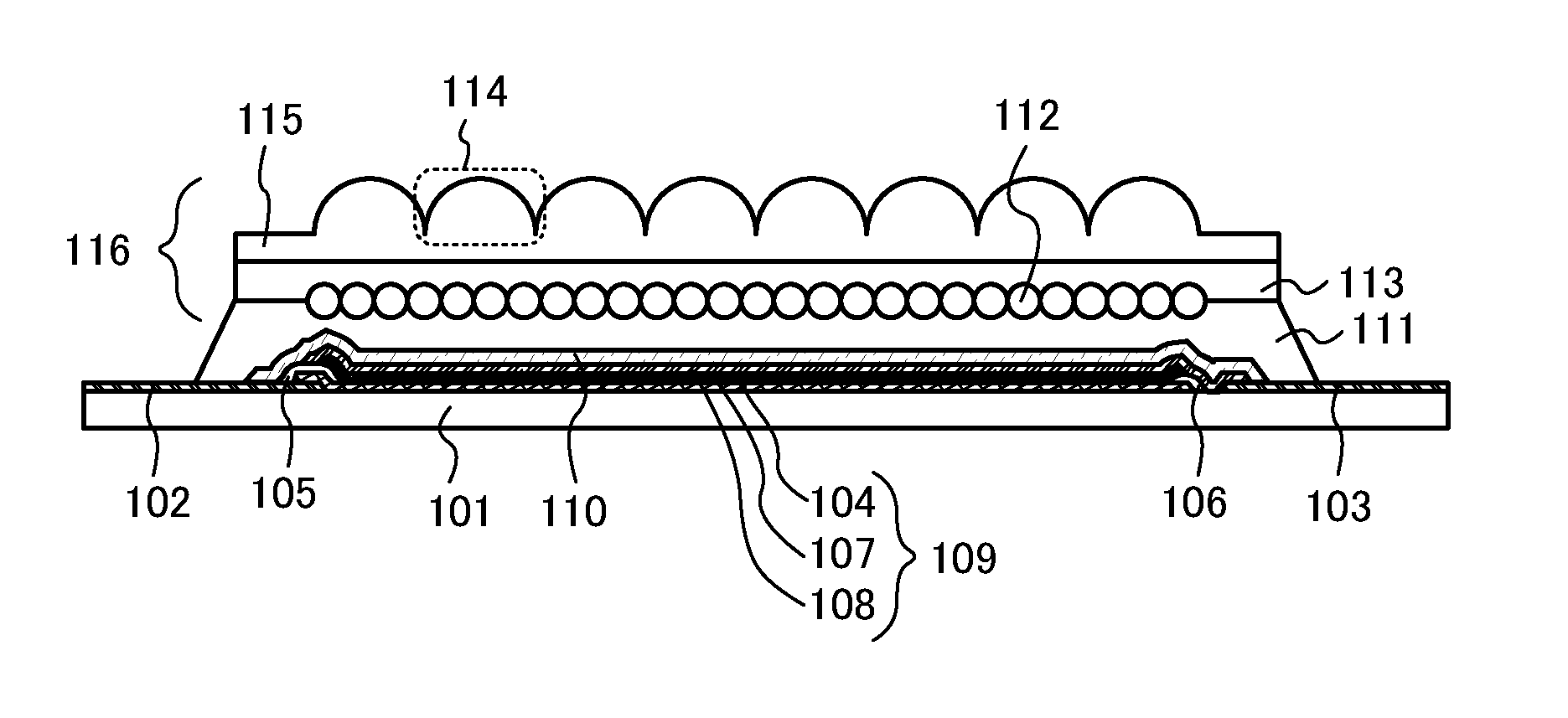
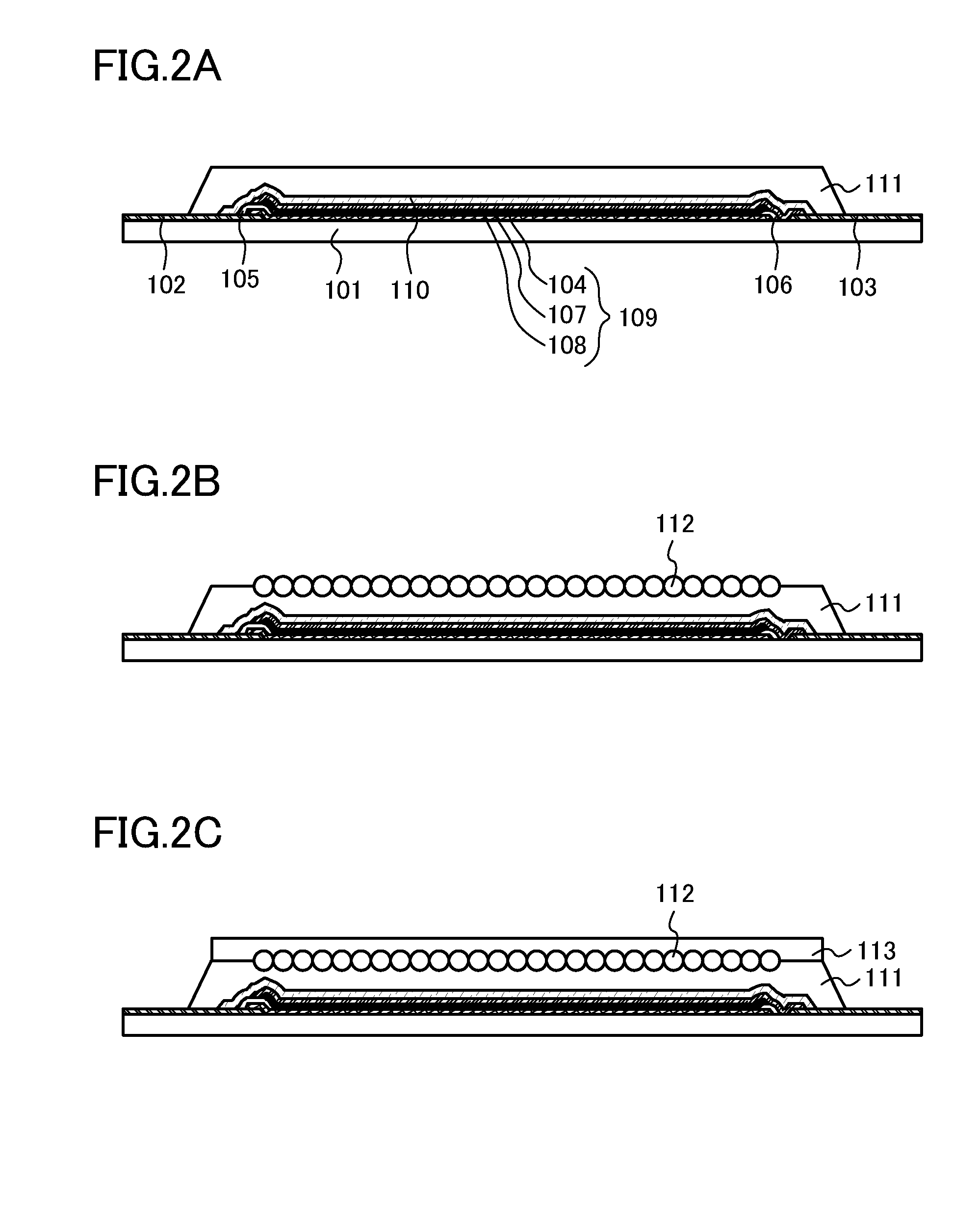
[0060]FIG. 1 shows a cross-sectional view of a lighting device of this embodiment. The lighting device shown in FIG. 1 includes a substrate 101, a first terminal 102, a second terminal 103, a first electrode 104 electrically connected to the first terminal 102, and a partition wall 105 and a partition wall 106 which are formed to cover edge portions of the first electrode 104. Further, the lighting device shown in FIG. 1 includes an EL layer 107 provided over the first electrode 104, the partition wall 105, and the partition wall 106, and a second electrode 108 provided over the EL layer 107 and the partition wall 106 and electrically connected to the second terminal 103. The first electrode 104, the EL layer 107, and the second electrode 108 form a light-emitting element layer 109.

[0061]Note that in the lighting device shown in FIG. 1, one light-emitting element layer 109 is provided as an example; however, the present invention is not limited to this. I...

embodiment 2

Structure of Lighting Device

[0141]FIG. 5 shows a cross-sectional view of a lighting device of this embodiment. The lighting device shown in FIG. 5 includes the substrate 101, the first terminal 102, the second terminal 103, the first electrode 104 electrically connected to the first terminal 102, and the partition wall 105 and the partition wall 106 which are formed to cover edge portions of the first electrode 104. Further, the lighting device shown in FIG. 5 includes the EL layer 107 provided over the first electrode 104, the partition wall 105, and the partition wall 106, and the second electrode 108 provided over the EL layer 107 and the partition wall 106 and electrically connected to the second terminal 103. The first electrode 104, the EL layer 107, and the second electrode 108 form the light-emitting element layer 109.

[0142]Note that in the lighting device shown in FIG. 5, one light-emitting element layer 109 is provided as an example; however, the present invention is not l...

embodiment 3

[0198]In this embodiment, structures of microlens arrays, methods for manufacturing the microlens array, and lighting devices, which are different from those in Embodiment 1 and Embodiment 2, will be described.

[0199]First, steps up to the manufacturing step shown in FIG. 2B, i.e., the steps of scattering the granules 112 over the resin layer 111 in an uncured state and curing the resin layer 111 are performed according to the description in Embodiment 1 (see FIG. 8A).

[0200]Next, a resin that is the material of the resin layer 113 in an uncured state is applied over the resin layer 111 in which the granule 112 is embedded (see FIG. 8B).

[0201]A plurality of granules 117 each having the diameter greater than that of the granule 112 is arranged over the uncured resin layer 113. Next, the resin layer 113 is cured (see FIG. 8C).

[0202]Through the above, the plurality of granules 112 is provided at the interface between the resin layer 111 and the resin layer 113. In addition, the plurality...


PUM


Abstract

The lighting device includes a first resin layer having a first refractive index and a second resin layer having a second refractive index lower than the first refractive index and higher than the refractive index of the air, which are over a light-emitting element layer, a plurality of granules provided at the interface between the first resin layer and the second resin layer and each having the second refractive index or a plurality of projections each having an apex provided inside the first resin layer and a flat surface in contact with the interface between the first resin layer and the second resin layer and having the second refractive index, an uneven structure provided at the interface with the air, and a resin substrate having the second refractive index.

Description

BACKGROUND OF THE INVENTION[0001]1. Field of the Invention[0002]One embodiment of the present invention relates to a lighting device and a method for manufacturing the lighting device.[0003]2. Description of the Related Art[0004]In recent years, development has been conducted on lighting using a light-emitting element which utilizes organic electroluminescence (EL) (hereinafter referred to as an organic EL light-emitting element). Since organic EL light-emitting elements can be formed in a film form, organic EL light-emitting elements can provide planar light emission and can be used as planar light sources. This is a distinctive feature that is difficult to obtain with a point light source typified by an incandescent lamp or an LED or a linear light source typified by a fluorescent lamp, and the utility value of organic EL light-emitting elements is high.[0005]However, in the case of a light-emitting element emitting light in a region with a higher refractive index than the air, su...

Claims


Application Information

Patent Timeline
Patent Type & Authority Applications(United States)
IPC IPC(8): H05B33/12B05D5/12
CPCG02B3/0025G02B5/0268H01L51/50H01L2251/10G02B5/0226H01L51/5253H01L51/5275H01L2251/5369H05B33/10G02B3/0056H01L51/5268H10K50/854H10K50/858H10K2102/331H01L33/58H10K50/844H10K50/00H10K71/00
Inventor HAMATANI, TOSHIJIADACHI, HIROKI
Owner SEMICON ENERGY LAB CO LTD
Why Eureka
Try Eureka