Method of Manufacturing Semiconductor Device Having Metal Gate

Active Publication Date: 2012-08-30
UNITED MICROELECTRONICS CORP
View PDF7 Cites 18 Cited by
  • Summary
  • Abstract
  • Description
  • Claims
  • Application Information

AI Technical Summary

Benefits of technology

[0009]The present invention uses organic materials as the first material layer or the second material layer, so a better filling result and a reliable CMP process can be prov

Problems solved by technology

However, with a trend toward scaling down the size of semiconductor devices, the conventional poly-silicon gate has faced problems such as inferior performance due to boron penetration and unavoidable depletion effect which increases equivalent thickness of the gat

Method used


Image

  • Method of Manufacturing Semiconductor Device Having Metal Gate
  • Method of Manufacturing Semiconductor Device Having Metal Gate
  • Method of Manufacturing Semiconductor Device Having Metal Gate

Examples


Example

[0014]To provide a better understanding of the presented invention, preferred embodiments will be made in detail. The preferred embodiments of the present invention are illustrated in the accompanying drawings with numbered elements.

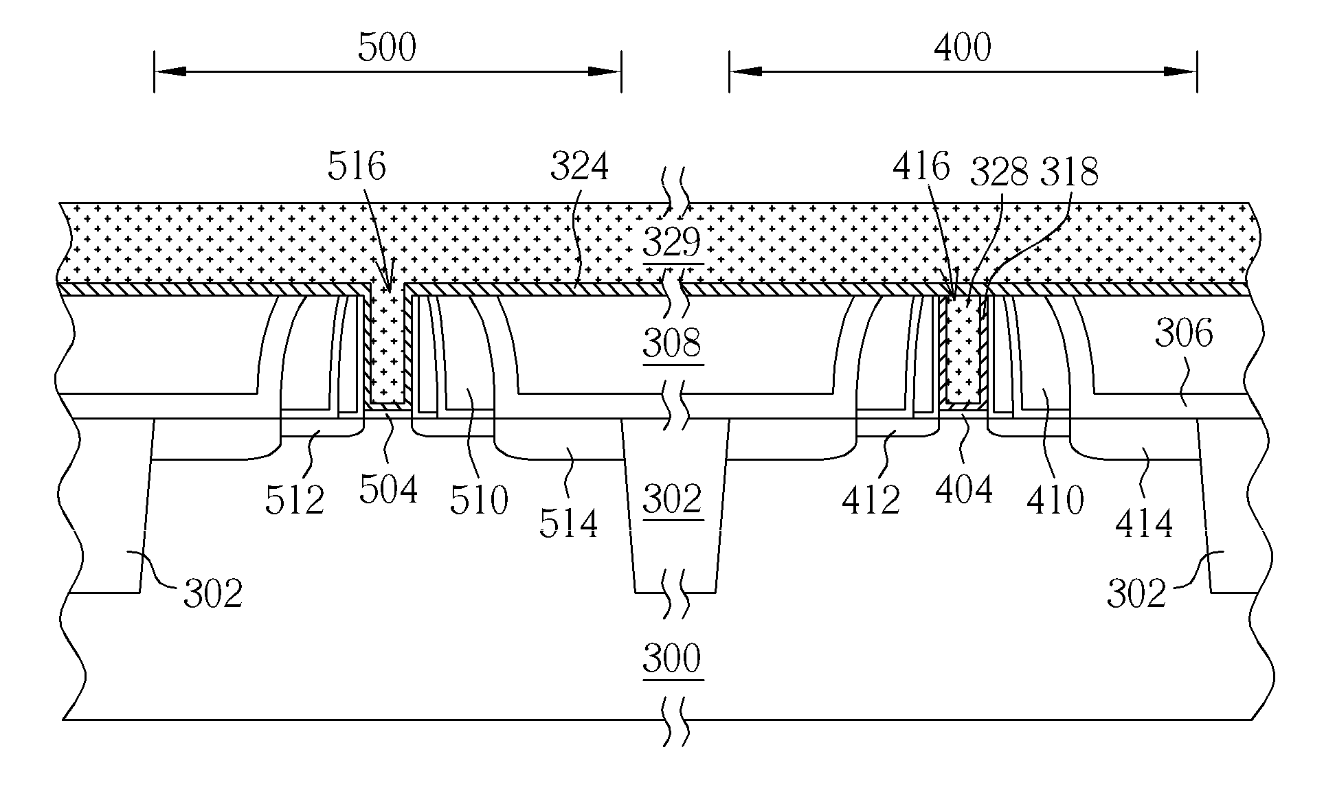
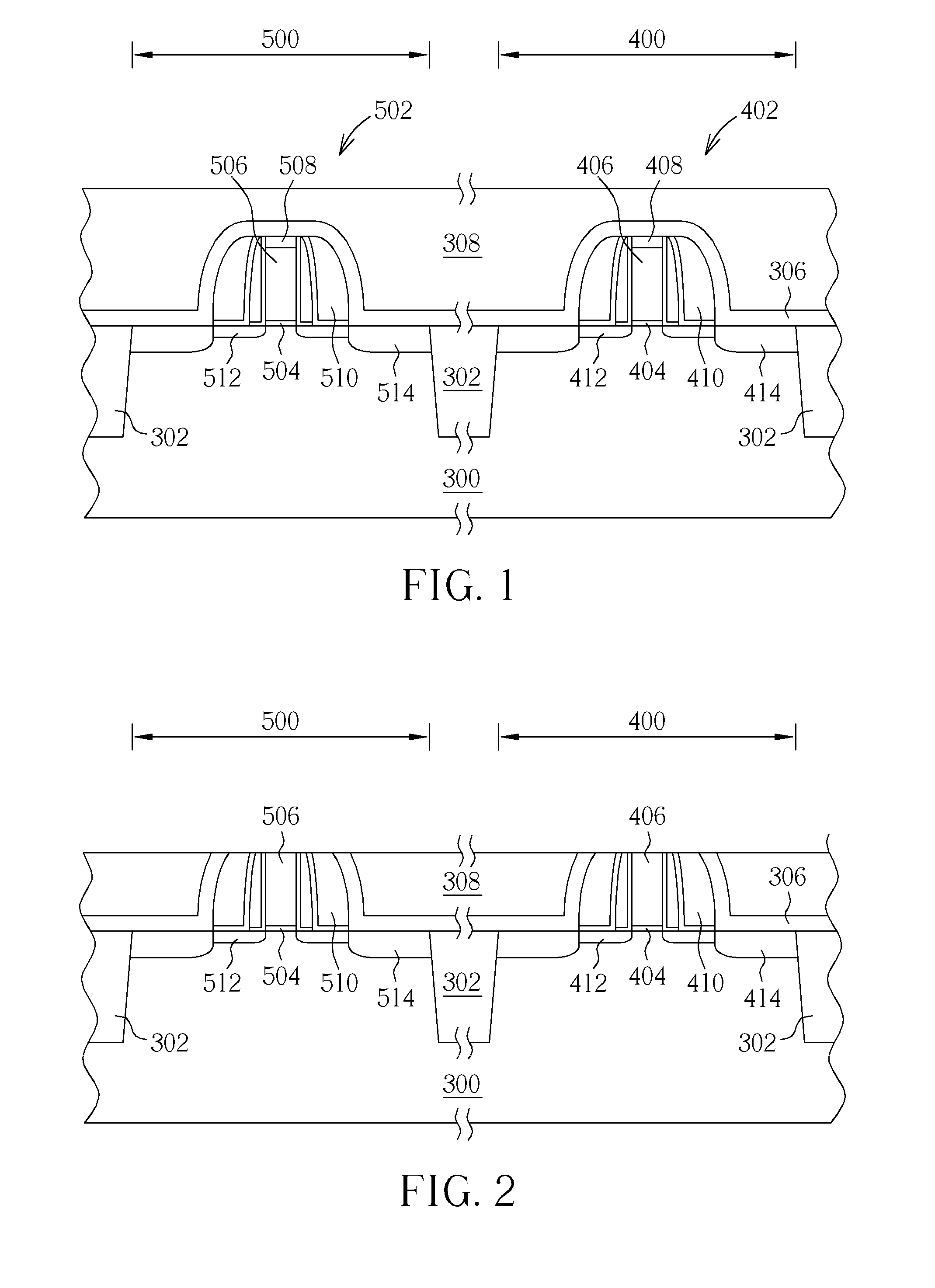
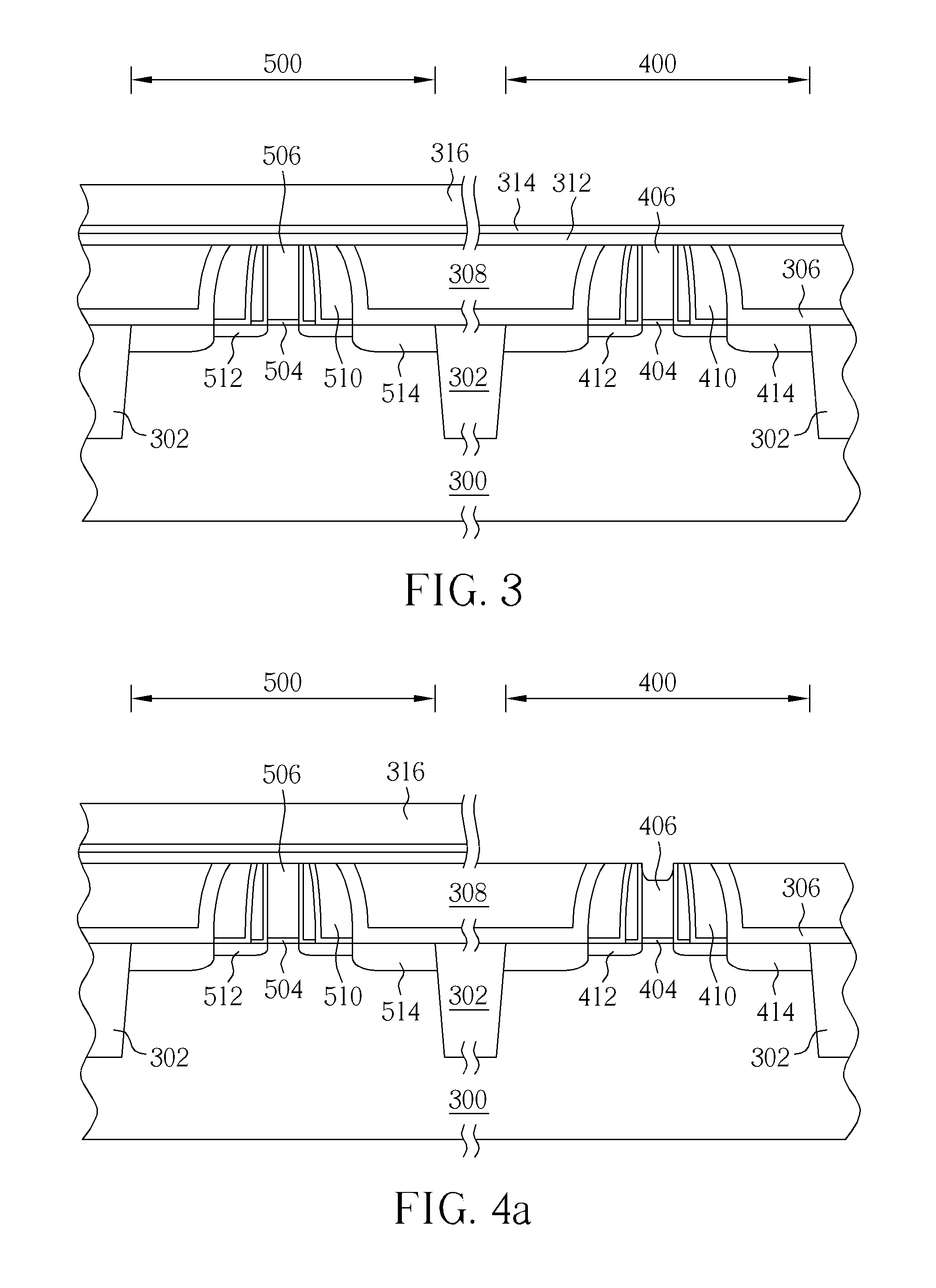
[0015]Please refer to FIG. 1 to FIG. 12, illustrating the schematic diagrams of the method of manufacturing the semiconductor device having metal gate according to the first embodiment of the present invention. First, a substrate 300 is provided, such as a silicon substrate, a silicon-containing substrate or a silicon-on-insulator (SOI) substrate. A plurality of shallow trench isolations (STI) 302 are disposed on the substrate 300. According to the areas encompassed by the STI 302, a first active region 400 and a second active region 500, which are insulated from each other, are defined on the substrate 300. Then, a first conductive type transistor 402 and a second conductive type transistor 502 are formed on the substrate 300 respectively in the first a...


PUM


Abstract

The present invention provides a method of manufacturing semiconductor device having metal gate. First, a substrate is provided. A first conductive type transistor having a first sacrifice gate and a second conductive type transistor having a second sacrifice gate are disposed on the substrate. The first sacrifice gate is removed to form a first trench and then a first metal layer and a first material layer are formed in the first trench. Next, the first metal layer and the first material layer are flattened. The second sacrifice gate is removed to form a second trench and then a second metal layer and a second material layer are formed in the second trench. Lastly, the second metal layer and the second material layer are flattened.

Description

BACKGROUND OF THE INVENTION[0001]1. Field of the Invention[0002]The present invention relates to a method of manufacturing a semiconductor device having a metal gate.[0003]2. Description of the Prior Art[0004]Poly-silicon is conventionally used as a gate electrode in semiconductor devices, such as the metal-oxide-semiconductor (MOS). However, with a trend toward scaling down the size of semiconductor devices, the conventional poly-silicon gate has faced problems such as inferior performance due to boron penetration and unavoidable depletion effect which increases equivalent thickness of the gate dielectric layer, reduces gate capacitance, and worsens a driving force of the devices. Therefore, work function metals are used to replace the conventional poly-silicon gate to be the control electrode that are suitable for use as the high-K gate dielectric layer.[0005]In a complementary metal-oxide semiconductor (CMOS) device, one of the dual work function metal gates is used in an NMOS de...

Claims


Application Information

Patent Timeline
IPC IPC(8): H01L21/28
CPCH01L21/82345H01L29/66545H01L29/4966H01L21/823842
Inventor LIAO, PO-JUITSAI, TSUNG-LUNGLIN, CHIEN-TINGHSU, SHAO-HUALU, SHUI-YENCHOU, PEI-YUCHEN, SHIN-CHILIAO, JIUNN-HSIUNGTSAI, SHANG-YUANYANG, CHAN-LONTSAI, TENG-CHUNLIN, CHUN-HSIEN
Owner UNITED MICROELECTRONICS CORP
Why Eureka
Try Eureka