Goa circuit based on oxide semiconductor thin film transistor

Active Publication Date: 2016-12-01
TCL CHINA STAR OPTOELECTRONICS TECH CO LTD
View PDF1 Cites 13 Cited by
  • Summary
  • Abstract
  • Description
  • Claims
  • Application Information

AI Technical Summary

Benefits of technology

The present invention provides a new design for a GOA circuit which addresses several issues that can affect the circuit's reliability and performance. The invention uses oxide semiconductor thin film transistor technology and includes several features to prevent electrical leakage, reduce crossfire current, and clear interference. The result is a more reliable and efficient GOA circuit that guarantees normal output of the image and display.

Problems solved by technology

Thus, the design difficulty of the GOA circuit based on the oxide semiconductor thin film transistor will be increased.
There will be some function issues happening when the design adaptable to the scan driving circuit for the amorphous silicon semiconductors is applied to the GOA circuit based on the oxide semiconductor thin film transistor.
Besides, due to some external factor inductions and the stress effect, there will be a tendency that the threshold voltage diminishes toward minus value to the oxide semiconductor thin film transistor, which may directly result in malfunction of the GOA circuit for the oxide semiconductor thin film transistors.
However, there are still some certain problems remaining in the GOA circuit based on oxide semiconductor thin film transistor according to prior art.

Method used


Image

  • Goa circuit based on oxide semiconductor thin film transistor
  • Goa circuit based on oxide semiconductor thin film transistor
  • Goa circuit based on oxide semiconductor thin film transistor

Examples


Embodiment Construction

[0057]For better explaining the technical solution and the effect of the present invention, the present invention will be further described in detail with the accompanying drawings and the specific embodiments.

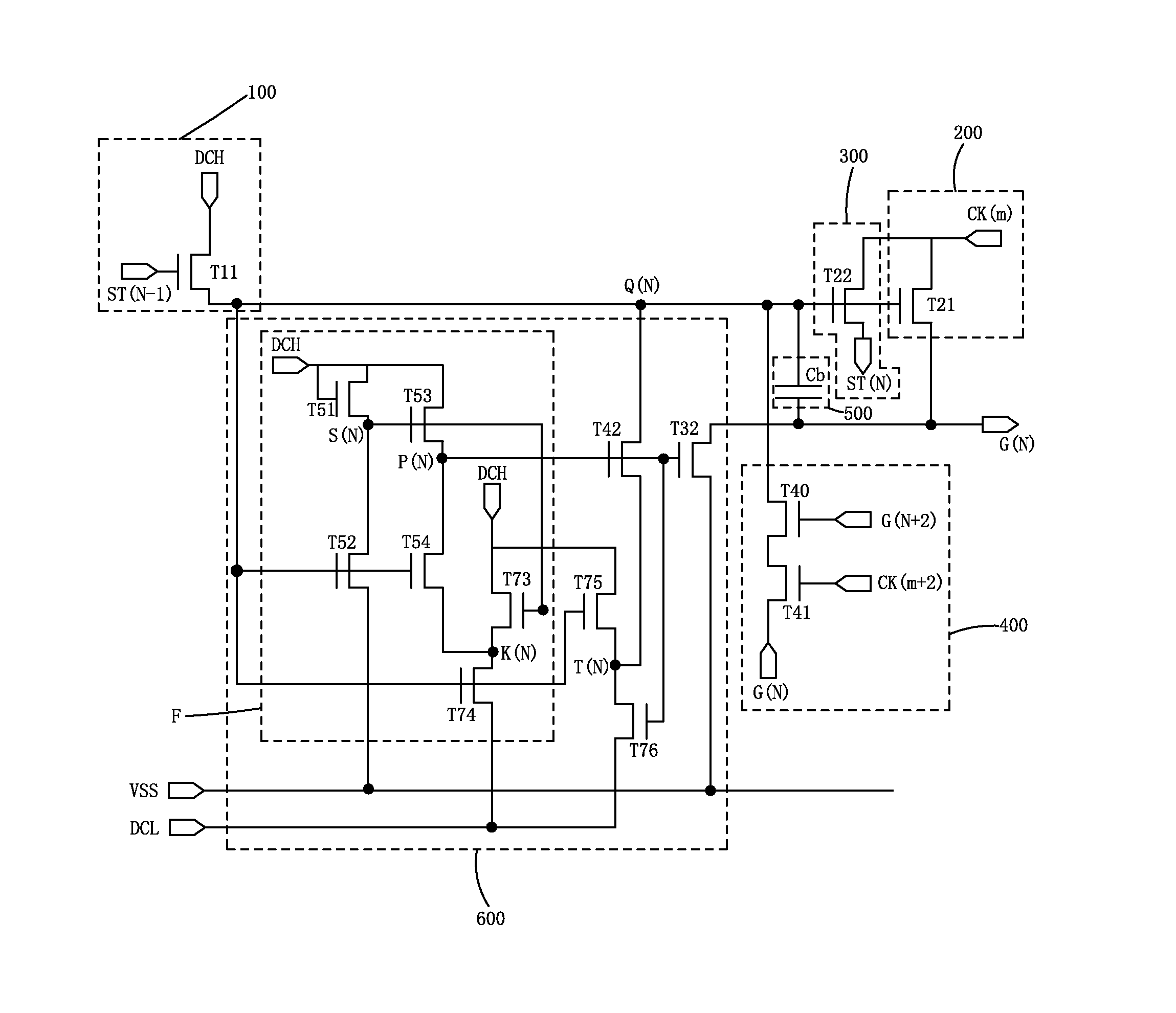
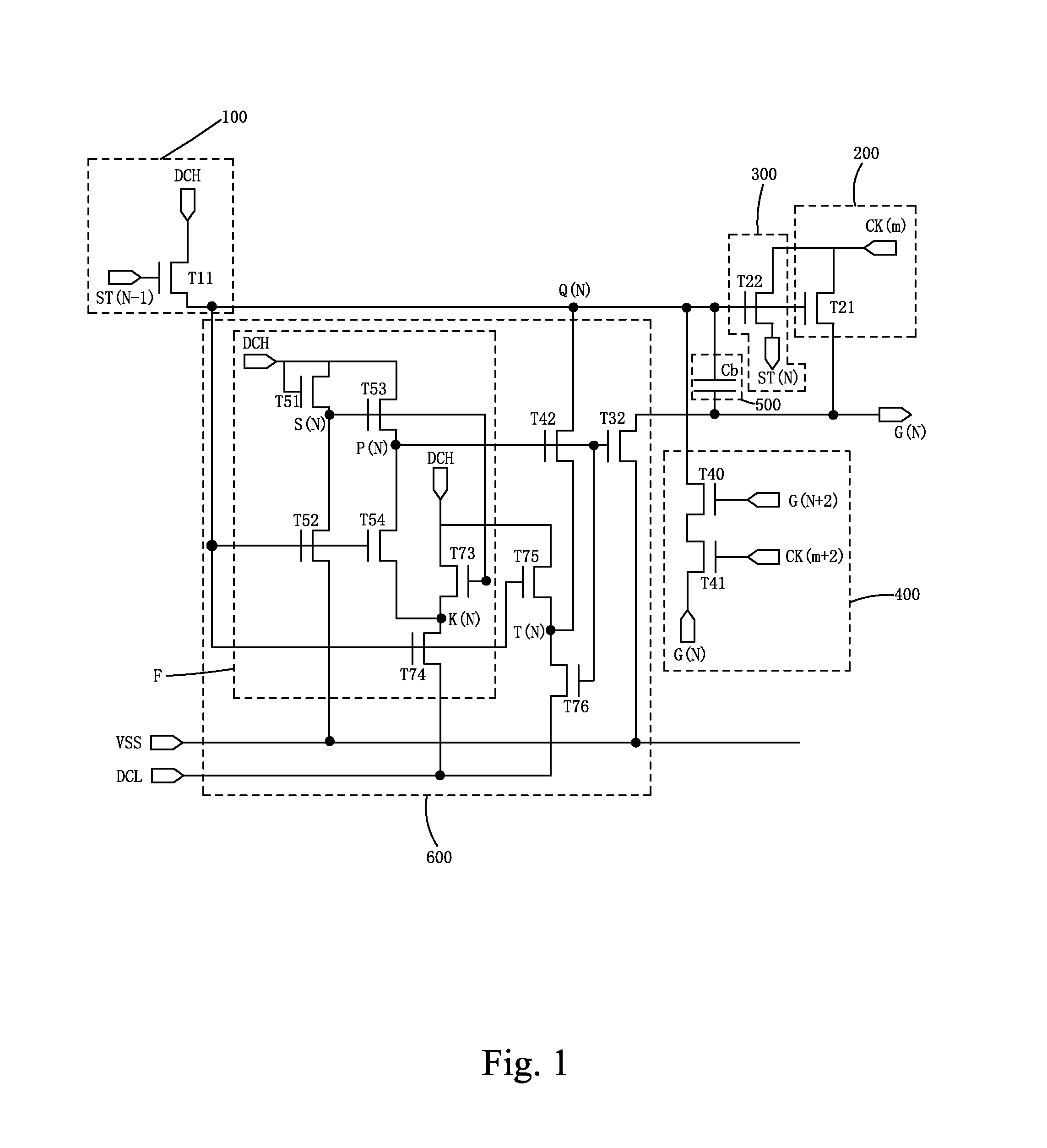
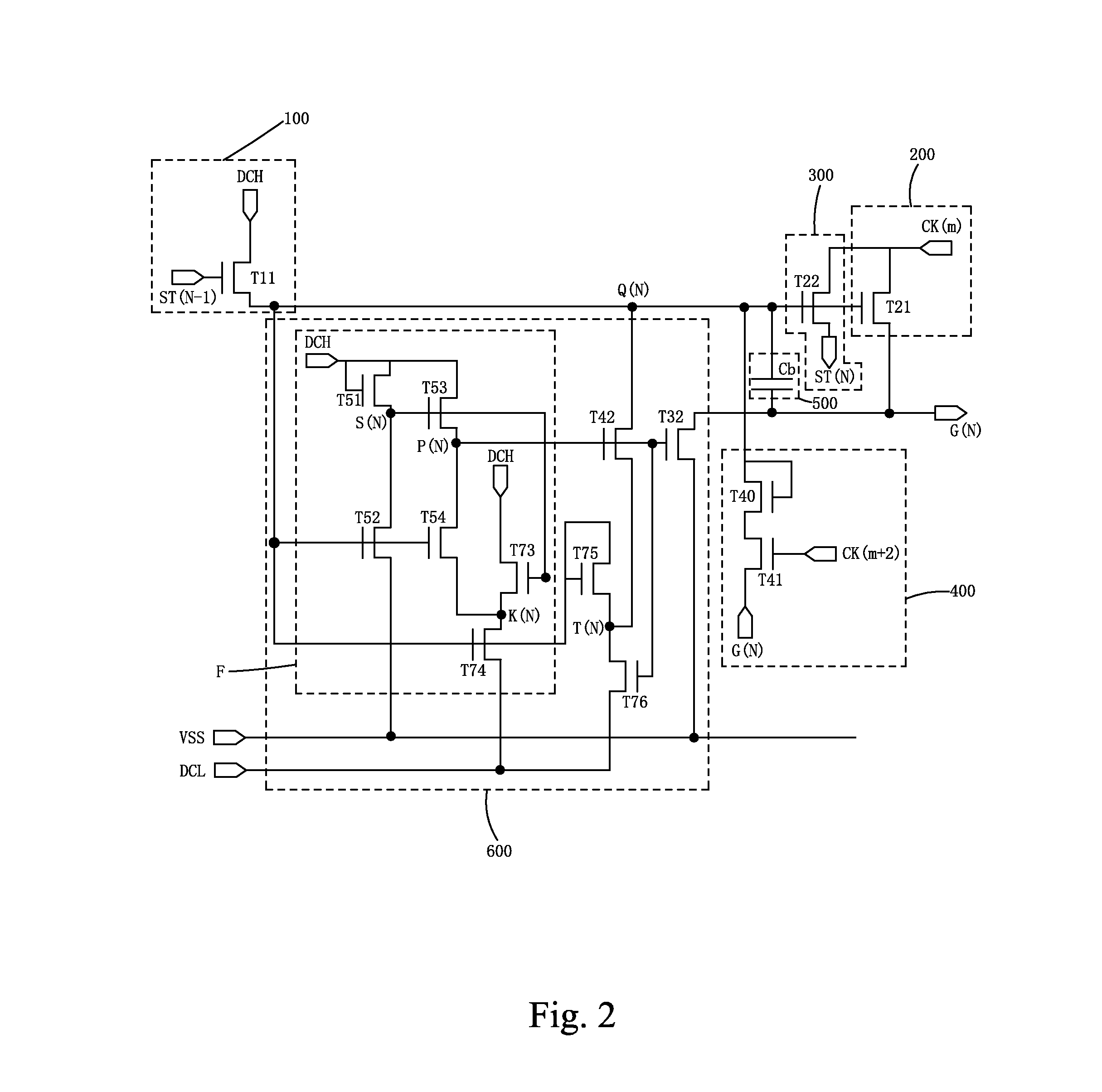
[0058]The present invention provides a GOA circuit based on oxide semiconductor thin film transistor. Please refer to FIG. 2, which is a circuit diagram of the first embodiment according to a GOA circuit based on oxide semiconductor thin film transistor of the present invention, comprising a plurality of GOA unit circuits which are cascade connected, and all the GOA unit circuit of every stage comprises a pull-up controlling module 100, a pull-up module 200, a transmission module 300, a first pull-down module 400, a bootstrap capacitor module 500 and a pull-down holding module 600.

[0059]N is set to be a positive integer and except the GOA unit circuit of the first stage, in the GOA unit circuit of the Nth stage:

[0060]the pull-up controlling module 100 comprises an eleventh thi...


PUM


Abstract

The present invention provides a GOA circuit based on oxide semiconductor thin film transistor, which cannot only prevent the electrical leakage to raise the reliability of the GOA circuit but also avoid the generation of the crossfire current in the non-function period by shorting the gate and the source of the fortieth thin film transistor (T40) in the first pull-down module (400) for avoiding the influence of the constant high voltage level (DCH) to the pull-down holding of the first node by electrically coupling both the gate and the drain of the seventy-fifth thin film transistor (T75) in the pull-down holding module (600) to the first node (Q(N)), and clearing the interference of the residual charge to the GOA circuit by providing the reset module (700) to reset the first node (Q(N)) before generating the each frame to guarantee the normal output of the GOA circuit and the normal display of the image.

Description

FIELD OF THE INVENTION[0001]The present invention relates to a display technology field, and more particularly to a GOA circuit based on oxide semiconductor thin film transistor.BACKGROUND OF THE INVENTION[0002]The Liquid Crystal Display (LCD) possesses advantages of thin body, power saving and no radiation to be widely used in many application scope, such as LCD TV, mobile phone, personal digital assistant (PDA), digital camera, notebook, laptop, and dominates the flat panel display field.[0003]Most of the liquid crystal displays on the present market are backlight type liquid crystal displays, which comprise a liquid crystal display panel and a backlight module. The working principle of the liquid crystal display panel is that the Liquid Crystal is injected between the Thin Film Transistor Array Substrate (TFT array substrate) and the Color Filter (CF). The light of backlight module is refracted to generate images by applying driving voltages to the two substrates for controlling ...

Claims


Application Information

Patent Timeline
IPC IPC(8): G09G3/36H01L27/12H01L29/786
CPCG09G3/3677H01L29/7869H01L27/1225G09G2320/0214G09G2310/061G09G2310/08H01L27/1255G09G3/3266
Inventor DAI, CHAO
Owner TCL CHINA STAR OPTOELECTRONICS TECH CO LTD
Why Eureka
Try Eureka