Method of manufacturing semiconductor wafer, and composite base and composite substrate for use in that method

a manufacturing method and semiconductor technology, applied in the field of manufacturing semiconductor wafers, can solve the problems of reducing efficiency, difficult to perform wet etching, and the method cannot be applied to the base, and achieve the effect of efficiently manufacturing the semiconductor wafer and efficiently manufacturing the semiconductor devi

Inactive Publication Date: 2012-09-13
SUMITOMO ELECTRIC IND LTD
View PDF3 Cites 14 Cited by
  • Summary
  • Abstract
  • Description
  • Claims
  • Application Information

AI Technical Summary

Benefits of technology

[0007]To solve the aforementioned problems and efficiently manufacture a semiconductor device, one object of the present invention is to provide a method of manufacturing a semiconductor wafer capable of efficiently manufacturing the semiconductor wafer regardless of the type of a base, and a composite base and a composite substrate suitably used in that manufacturing method.
[0015]According to the present invention, a method of manufacturing a semiconductor wafer capable of efficiently manufacturing the semiconductor wafer regardless of the type of a base, and a composite base and a composite substrate suitably used in that manufacturing method can be provided to efficiently manufacture a semiconductor device.

Problems solved by technology

Since the base is removed by wet etching in a method disclosed in Japanese Patent Laying-Open No. 2003-165798, there are problems that the method requires a long period of time to remove the base, causing a reduction in efficiency, and that the method cannot be applied to a base for which it is difficult to perform wet etching.

Method used


Image

  • Method of manufacturing semiconductor wafer, and composite base and composite substrate for use in that method
  • Method of manufacturing semiconductor wafer, and composite base and composite substrate for use in that method
  • Method of manufacturing semiconductor wafer, and composite base and composite substrate for use in that method

Examples


embodiment 1

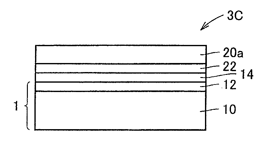
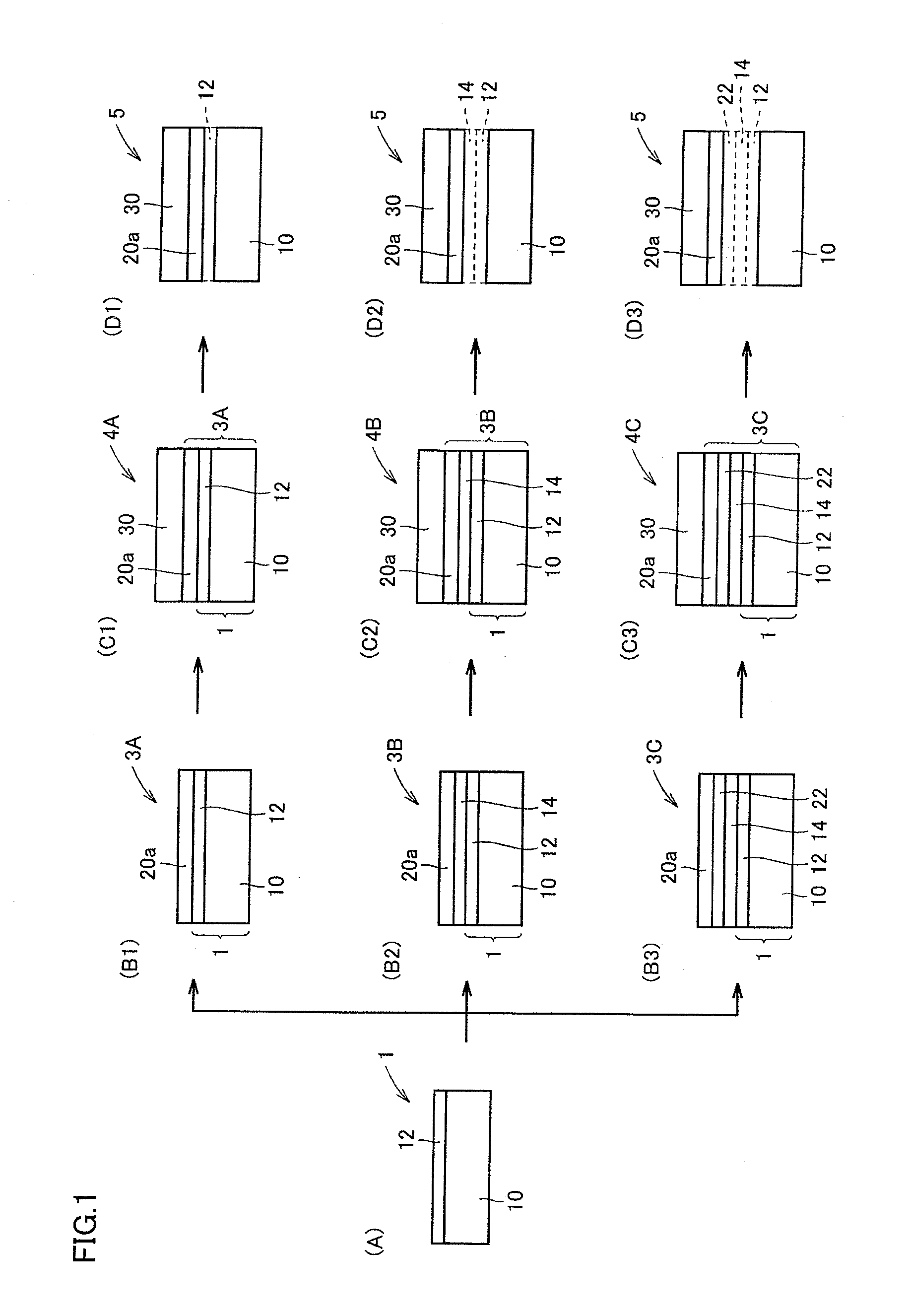
[0023]Referring to FIG. 1, a method of manufacturing a semiconductor wafer as one embodiment of the present invention includes the step of obtaining a composite base 1 by forming a base surface flattening layer 12 having a surface RMS roughness of not more than 1.0 nm on a base 10 (FIG. 1(A)), the step of obtaining a composite substrate 3A, 3B, 3C by attaching a semiconductor crystal layer 20a to a side of composite base 1 where base surface flattening layer 12 is located (FIG. 1(B1), (B2), and (B3)), the step of growing at least one semiconductor layer 30 on semiconductor crystal layer 20a of composite substrate 3A, 3B, 3C (FIG. 1(C1), (C2), and (C3)), and the step of obtaining a semiconductor wafer 5 including semiconductor crystal layer 20a and semiconductor layer 30 by removing base surface flattening layer 12 by wet etching and thereby separating semiconductor crystal layer 20a from base 10 (FIG. 1(D1), (D2), and (D3)). With the method of manufacturing a semiconductor wafer in ...

embodiment 2

Composite Base

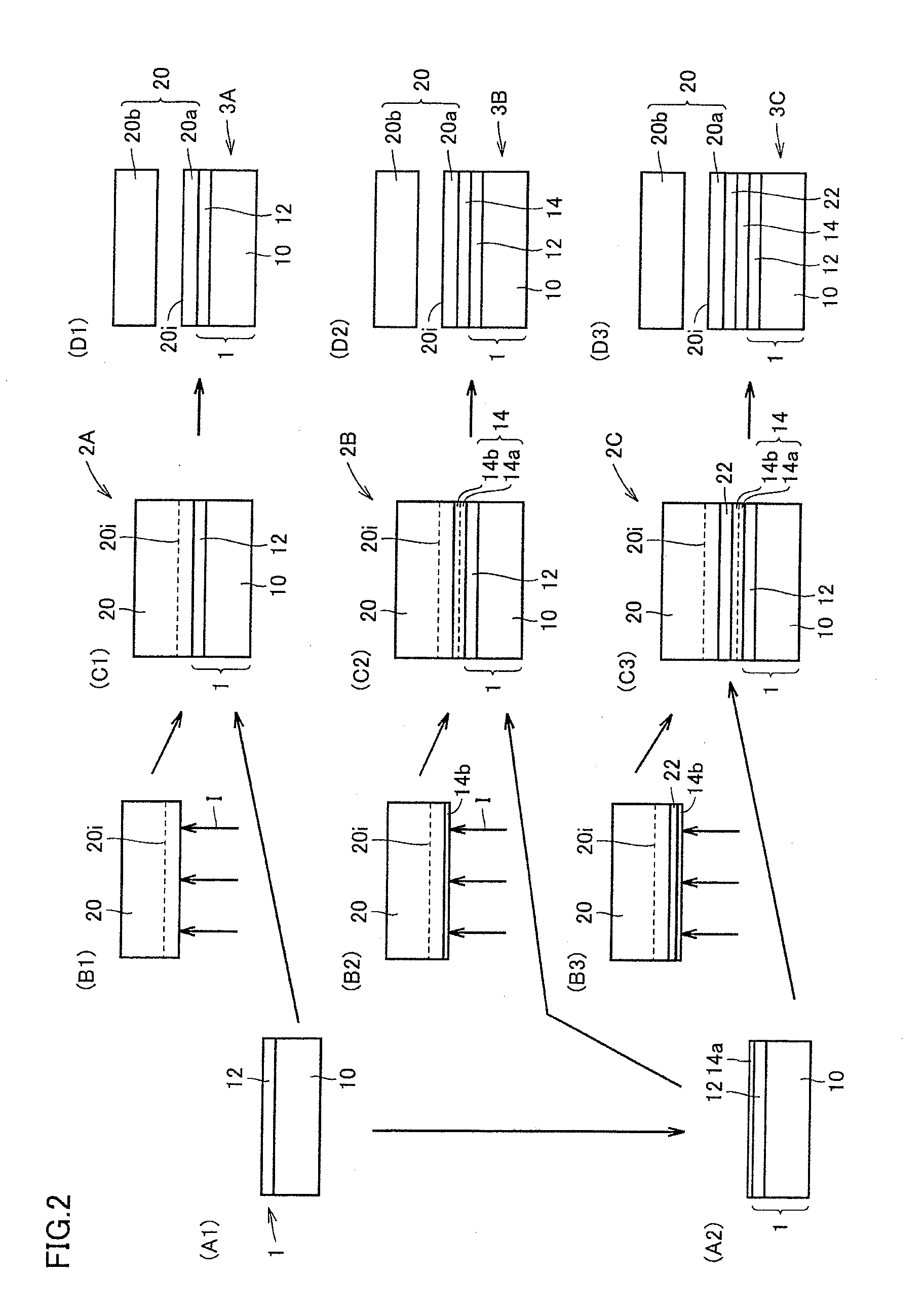
[0072]Referring to FIG. 3, composite base 1 as another embodiment in accordance with the present invention includes base 10, and base surface flattening layer 12 disposed on base 10. Base surface flattening layer 12 has a surface RMS roughness of not more than 1.0 nm, and a thickness of not less than 0.1 μm and not more than 50 μm. Since base surface flattening layer 12 disposed on base 10 has a surface RMS roughness of not more than 1.0 nm in composite base 1 in the present embodiment, a composite substrate can be obtained by attaching a semiconductor crystal layer to base surface flattening layer 12. Further, since the base surface flattening layer in composite base 1 in the present embodiment has a thickness of not less than 0.1 μm and not more than 50 μm, it can be easily removed by wet etching.

[0073](Base)

[0074]Although base 10 in composite base 1 in the present embodiment is not particularly limited, it preferably includes at least one selected from the group con...

embodiment 3

Composite Substrate

[0079]Referring to FIGS. 4 to 6, composite substrate 3A, 3B, 3C as still another embodiment of the present invention includes composite base 1 in Embodiment 2, and semiconductor crystal layer 20a disposed on the side of composite base 1 where base surface flattening layer 12 is located. The difference between the thermal expansion coefficient of base 10 and the thermal expansion coefficient of the semiconductor crystal layer is not more than 4.5×10⁻⁶K−1.

[0080]Since composite substrate 3A, 3B, 3C in the present embodiment has a high bondability between composite base 1 and semiconductor crystal layer 20a, and has a small difference between the thermal expansion coefficient of base 10 in composite base 1 and the thermal expansion coefficient of semiconductor crystal layer 20a of not more than 4.5×10⁻⁶K−1, a semiconductor layer with high crystallinity can be epitaxially grown on semiconductor crystal layer 20a of composite substrate 3A, 3B, 3C without occurrence of c...


PUM

PropertyMeasurementUnit
surface RMS roughnessaaaaaaaaaa
thicknessaaaaaaaaaa
thicknessaaaaaaaaaa

Abstract

A method of manufacturing a semiconductor wafer of the present invention includes the steps of: obtaining a composite base by forming a base surface flattening layer having a surface RMS roughness of not more than 1.0 nm on a base; obtaining a composite substrate by attaching a semiconductor crystal layer to a side of the composite base where the base surface flattening layer is located; growing at least one semiconductor layer on the semiconductor crystal layer of the composite substrate; and obtaining the semiconductor wafer including the semiconductor crystal layer and the semiconductor layer by removing the base surface flattening layer by wet etching and thereby separating the semiconductor crystal layer from the base. Thus, a method of manufacturing a semiconductor wafer capable of efficiently manufacturing the semiconductor wafer regardless of the type of a base, and a composite base and a composite substrate suitably used in that manufacturing method are provided to efficiently manufacture a semiconductor device.

Description

BACKGROUND OF THE INVENTION[0001]1. Field of the Invention[0002]The present invention relates to a method of manufacturing a semiconductor wafer, and a composite base and a composite substrate for use in that method.[0003]2. Description of the Background Art[0004]Manufacturing a wafer including a semiconductor crystal layer and a semiconductor layer by forming a composite substrate in which the semiconductor crystal layer is attached to a different composition base having a chemical composition different from that of the semiconductor crystal layer, growing the semiconductor layer on the semiconductor crystal layer of the composite substrate, and thereafter removing the different composition base has been proposed to efficiently manufacture a semiconductor device.[0005]For example, Japanese Patent Laying-Open No. 2003-165798 discloses manufacturing a wafer including a single crystal sapphire substrate and a gallium nitride single crystal by attaching the single crystal sapphire subs...

Claims


Application Information

Patent Timeline
Patent Type & Authority Applications(United States)
IPC IPC(8): H01L29/04B32B3/00H01L27/12H01L29/02H01L21/762H01L29/22
CPCY10T428/24355H01L21/76254B32B2307/704B32B2264/102Y10T428/264H01L29/0684B32B2457/14
Inventor SEKI, YUKISATOH, ISSEIUEMATSU, KOJIYAMAMOTO, YOSHIYUKI
Owner SUMITOMO ELECTRIC IND LTD
Why Eureka
Try Eureka