Semiconductor integrated circuit, failure diagnosis system and failure diagnosis method

a technology of integrated circuits and failure diagnosis systems, applied in the field of failure diagnosis systems and memory devices, can solve the problems of not being suitable for practical use, taking a long time to fully generate a failure bit map,

Inactive Publication Date: 2012-09-13
KK TOSHIBA
View PDF3 Cites 7 Cited by
  • Summary
  • Abstract
  • Description
  • Claims
  • Application Information

AI Technical Summary

Problems solved by technology

Unfortunately, in on-line information collection for each wafer or lot by means of BIST circuits during mass

Method used


Image

  • Semiconductor integrated circuit, failure diagnosis system and failure diagnosis method
  • Semiconductor integrated circuit, failure diagnosis system and failure diagnosis method
  • Semiconductor integrated circuit, failure diagnosis system and failure diagnosis method

Examples


first embodiment

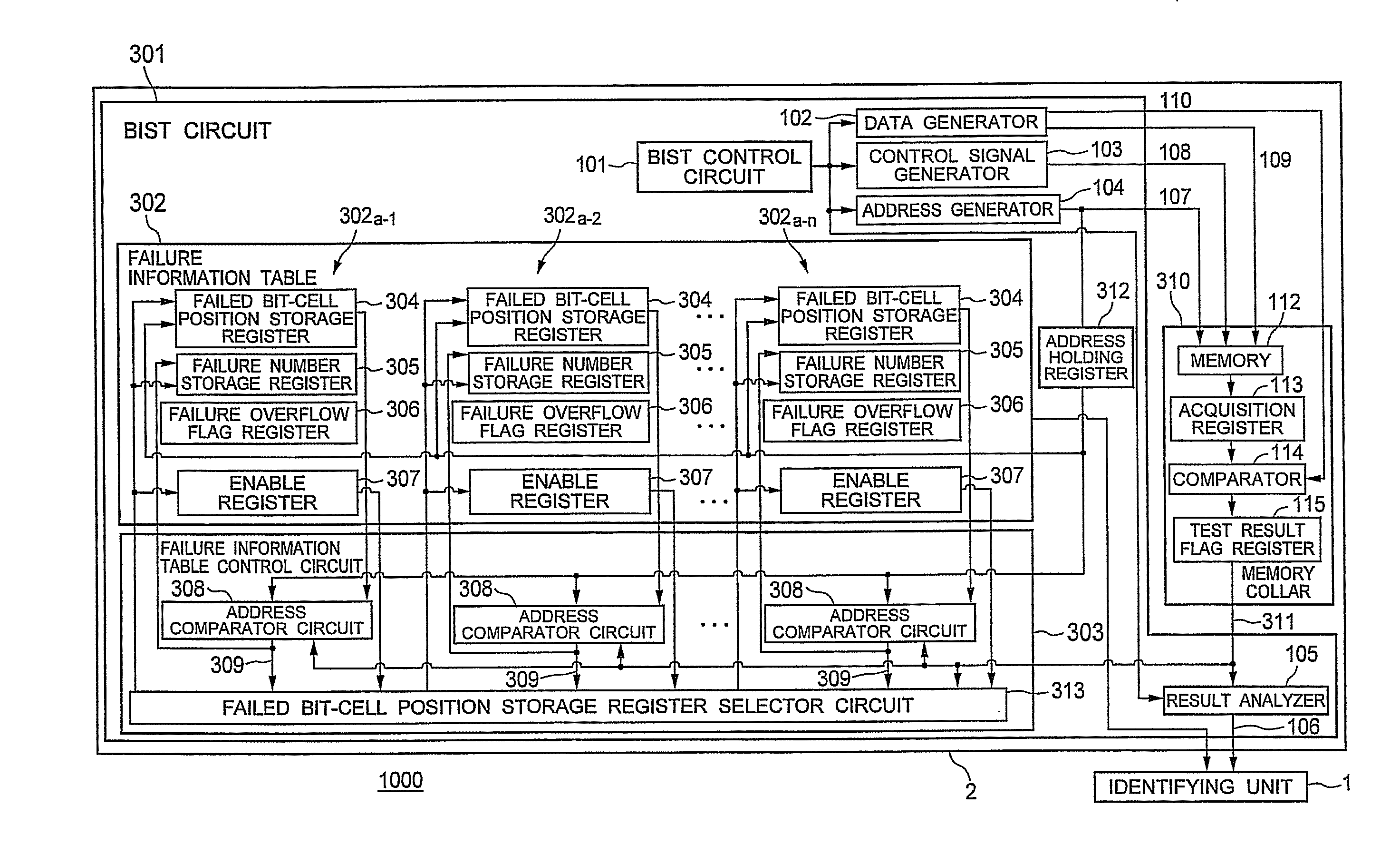
[0019]FIG. 1 shows an example of the configuration of a failure analysis system 1000 according to a first embodiment.

[0020]As shown in FIG. 1, the failure analysis system 1000 includes an identifying unit 1 and a semiconductor integrated circuit 2.

[0021]The semiconductor integrated circuit 2 includes: a built-in self-test (BIST) circuit 301 that diagnoses memory failures; and a memory collar 310.

[0022]The BIST circuit 301 includes a BIST control circuit 101, a data generator 102, a control signal generator 103, an address generator 104, a result analyzer 105, a failure information table 302, a failure information table control circuit 303, and an address holding register 312.

[0023]The BIST control circuit 101 controls the data generator 102, the control signal generator 103, and the address generator 104 to sequentially generate necessary signals, so that the BIST control circuit 101 controls a BIST on a memory 112.

[0024]The data generator 102 is controlled by the BIST control circu...

second embodiment

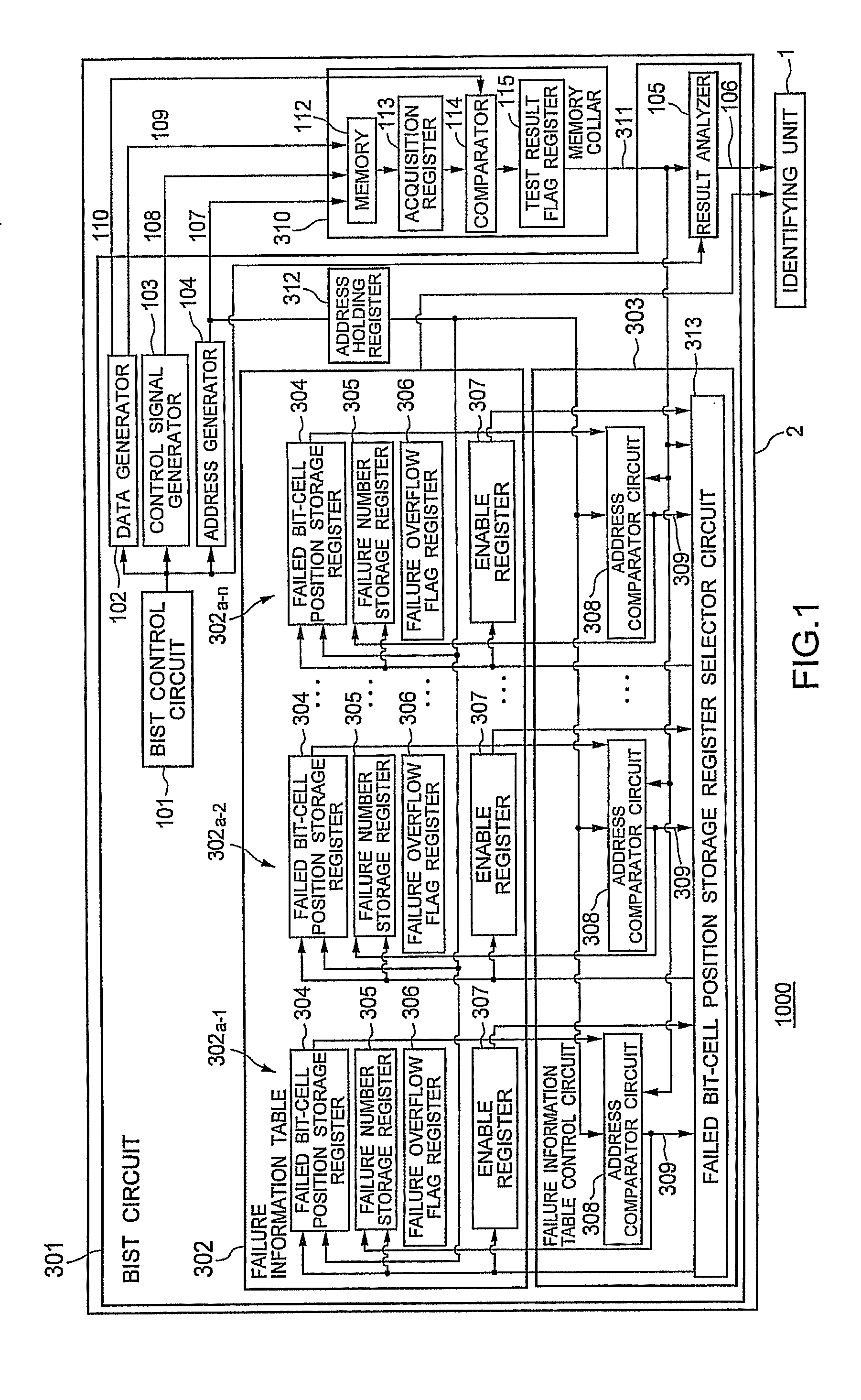
[0064]A second embodiment will describe a structural example in which the BIST circuit of the first embodiment further includes a configuration for outputting a table overflow flag indicating that failure data exceeds a data amount storable in a failure information table.

[0065]FIG. 2 shows an example of the configuration of a failure diagnosis system 2000 according to the second embodiment. In FIG. 2, the same reference numerals as in FIG. 1 indicate the same configurations as in the first embodiment. Some of the constituent elements of a failure information table 302 are omitted in FIG. 2 but the failure information table 302 is identical in configuration to that of FIG. 1. Moreover, in a failure information table control circuit 303a, the failed bit-cell position storage register selector circuit 313 included in the failure information table control circuit 303 of FIG. 1 is omitted.

[0066]As shown in FIG. 2, the failure diagnosis system 2000 includes an identifying unit 1 and a sem...

third embodiment

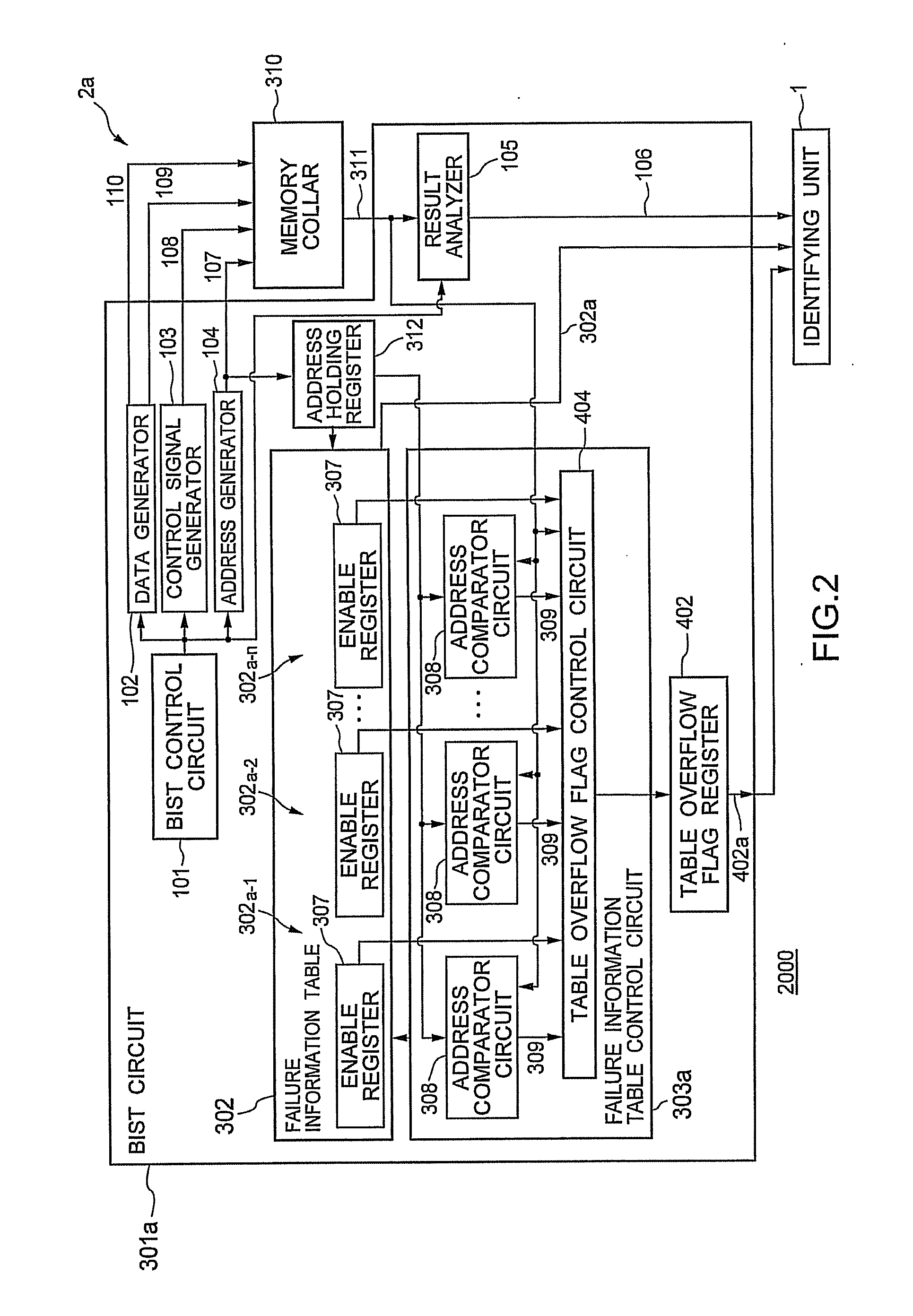
[0080]A third embodiment will describe a structural example in which the BIST circuit of the second embodiment further includes a configuration for switching the modes of a failure information table.

[0081]FIG. 3 shows an example of the configuration of a failure diagnosis system 3000 according to the third embodiment. In FIG. 3, the same reference numerals as in FIG. 2 indicate the same configurations as in the second embodiment. Some of the constituent elements of a failure information table 302 and a failure information table control circuit 303a are omitted in FIG. 3 but the failure information table 302 is identical in configuration to that of FIG. 1 and the failure information table control circuit 303a is identical to that of FIG. 2.

[0082]As shown in FIG. 3, the failure diagnosis system 3000 includes an identifying unit 1 and a semiconductor integrated circuit 2b.

[0083]Unlike the BIST circuit 301a of the second embodiment, a BIST circuit 301b further includes a table mode swi...


PUM


Abstract

A semiconductor integrated circuit includes a memory containing multiple memory bits that store predetermined data placed in a first address direction and a second address direction. The semiconductor integrated circuit includes a BIST (Built-in Self-Test) circuit that diagnoses a failure of the memory.
The BIST circuit includes a BIST control circuit that controls a BIST on the memory. The BIST circuit includes a failure information table storing: a failed bit-cell position that is an address of a bit cell identified in the first address direction as a failed bit cell by the BIST conducted in the first address direction; the number of bit cell failures at the failed bit-cell position; and a failure overflow flag indicating whether the number of failures exceeds a predetermined upper value or not. The BIST circuit includes a result analyzer that outputs a BIST result obtained by the BIST on the memory.

Description

CROSS-REFERENCE TO RELATED APPLICATION[0001]This application is based upon and claims the benefit of priority from the prior Japanese Patent Application No. 2011-050210, filed on Mar. 8, 2011, the entire contents of which are incorporated herein by reference.BACKGROUND[0002]1. Field[0003]Embodiments described herein relate generally to a failure diagnosis system diagnosing a memory device mounted in a semiconductor integrated circuit.[0004]2. Background Art[0005]In a method of detecting failures in a manufacturing test according to the related art, a built-in self-test (BIST) circuit is incorporated into a memory device mounted in a semiconductor integrated circuit.[0006]Such failure detection methods include a comparator-type BIST in which written data and read data are compared to each other to decide the presence or absence of failures and a compressor-type BIST in which read results are compressed in a BIST circuit and the presence or absence of failures is decided based on the ...

Claims


Application Information

Patent Timeline
IPC IPC(8): G01R31/3187
CPCG11C29/16G11C29/44G11C2029/4402G11C2029/1208G11C2029/0401
Inventor ANZOU, KENICHITOKUNAGA, CHIKAKOMORISHIMA, SHOHEI
Owner KK TOSHIBA
Why Eureka
Try Eureka