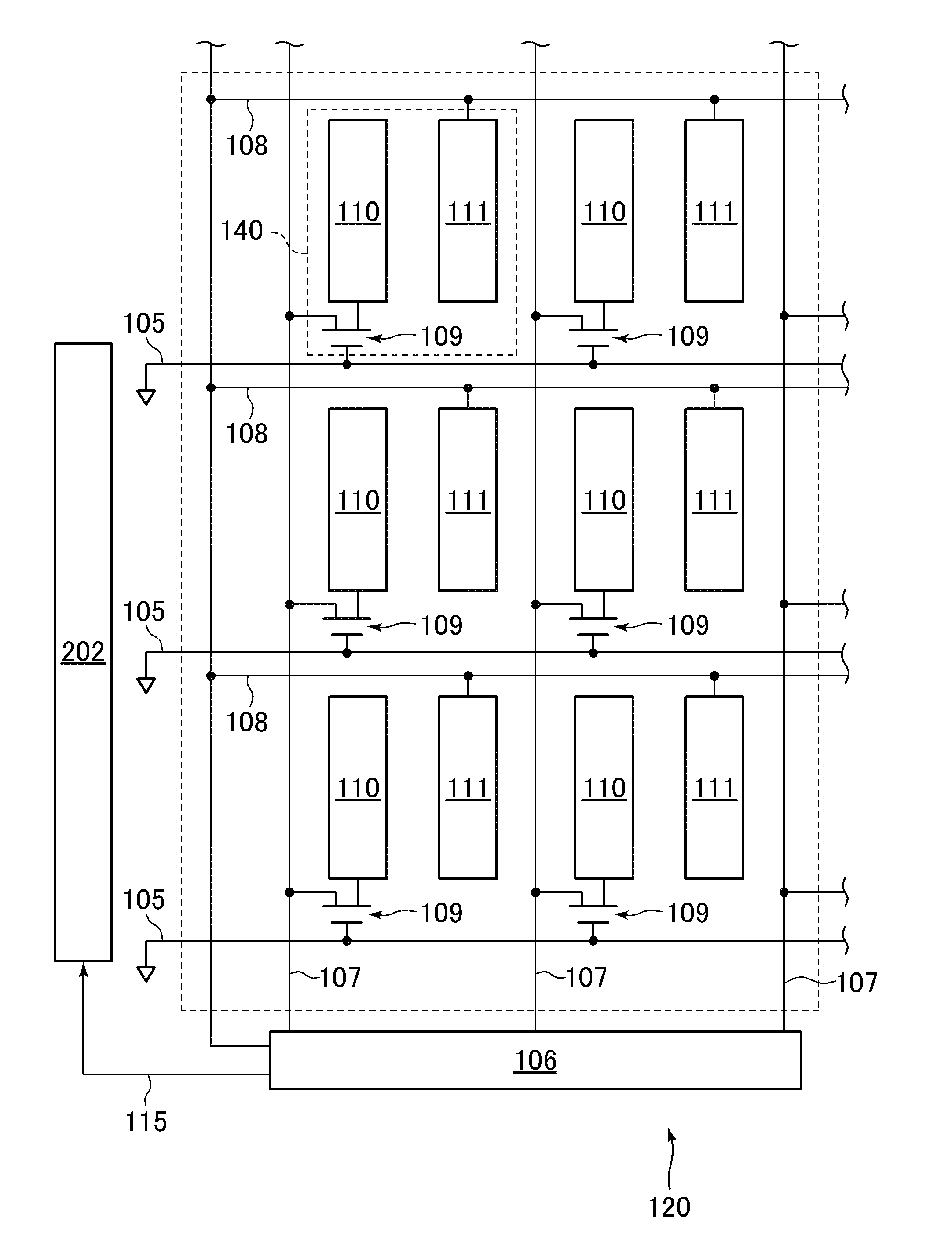
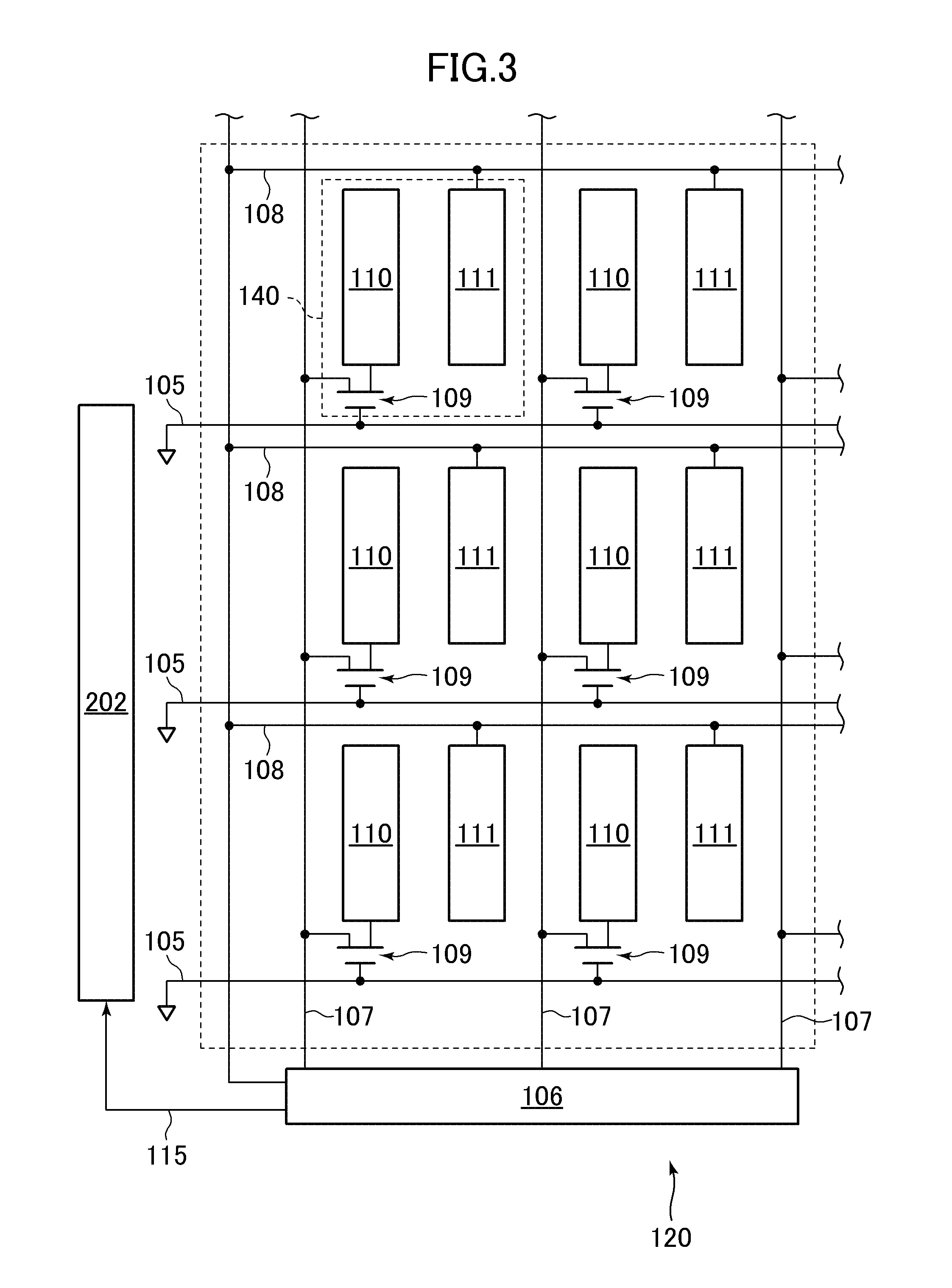
Display device

a technology of display device and gate circuit, which is applied in the field of display device having gate circuit, can solve problems such as deterioration of display quality

Active Publication Date: 2012-09-13
JAPAN DISPLAY INC
View PDF10 Cites 18 Cited by
  • Summary
  • Abstract
  • Description
  • Claims
  • Application Information

AI Technical Summary

Benefits of technology

[0027]In light of the problems as explained above, and an object of one or more embodiments of the present invention is to provide a display device which suppresses influence by a difference in storage voltages of the pixel circuit 130, occurring in a case of forward scanning driving and in a case of backward scanning driving, and improves display quality.
[0034](7) In the display device set forth in any one of (1) to (6), the n-th basic circuit further includes a bootstrap circuit that further increases a high voltage value of the first node according to a high voltage level of the m-th clock signal.

Problems solved by technology

However, in the gate circuit performing bidirectional scanning driving, parasitic capacitance between the gate and source, which is generated in the transistor included in the pixel circuit, may be different between in the case of performing forward scanning driving and in the case of performing backward scanning driving.
The voltage of the pixel electrode with respect to a reference electrode becomes different, and thus display quality is deteriorated.

Method used


Image

  • Display device
  • Display device
  • Display device

Examples


modified example

[0086]Next, a modified example of the present invention will be described. The modified example is different from the embodiment explained above in that overlap driving of three horizontal periods is performed, three gate circuits are used according thereto, and the three gate circuits are divided and disposed at left and right sides. In addition, in the following, description of the similar configuration as in the embodiment will be omitted.

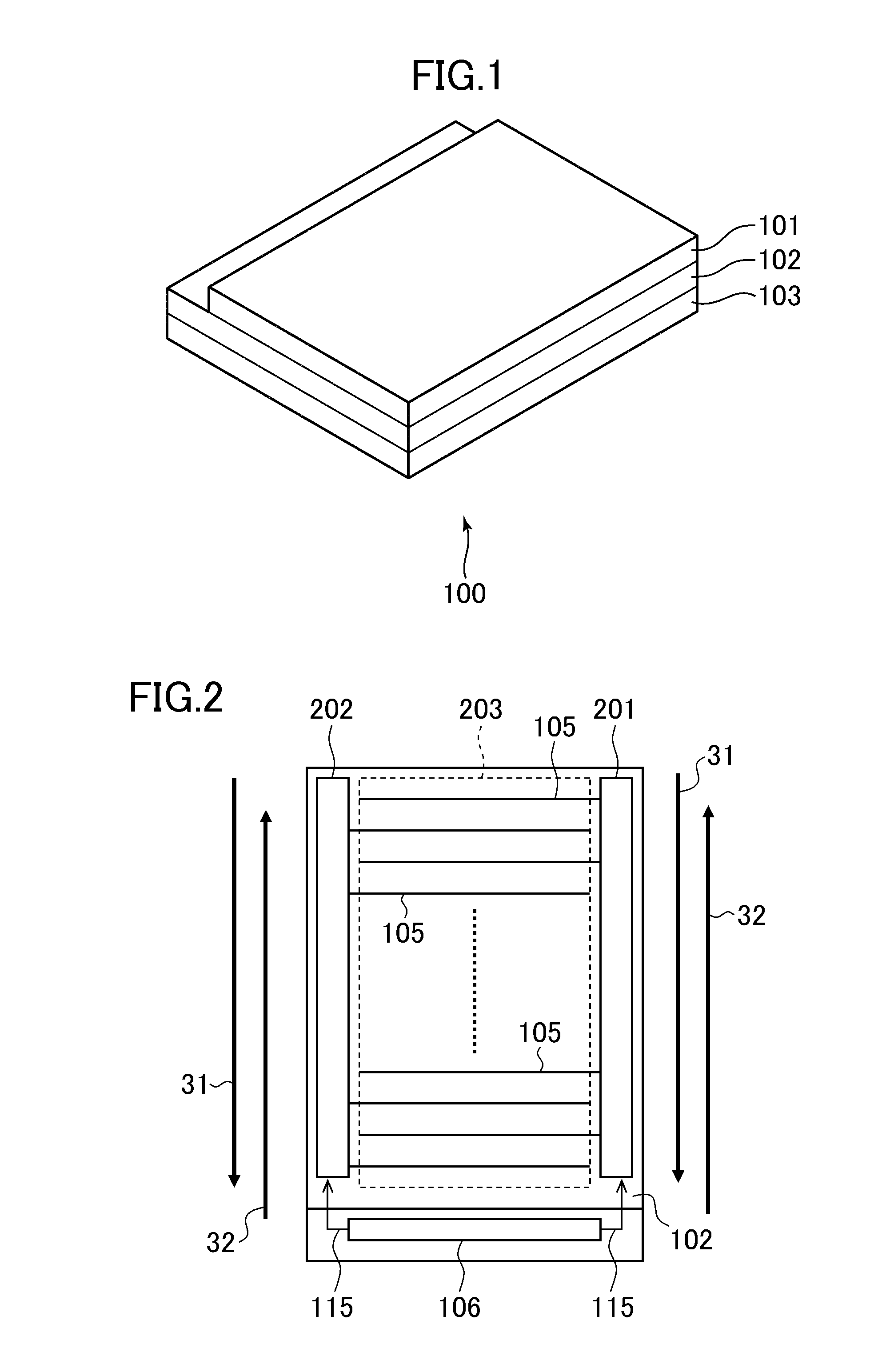
[0087]FIG. 8 is a diagram illustrating an outline of disposition of the gate circuits according to the modified example. In the same manner as the embodiment, a display device 800 according to the modified example includes a display portion 203, a driver 106, and gate circuits 801, 802 and 803. However, in the gate circuits 801, 802 and 803 according to the modified example, for example, in a case of forward scanning, the first gate circuits 801 output a gate signal to the k-th gate line 105, the second gate circuits 802 output a gate signal to ...


PUM


Abstract

A display device includes a plurality of pixel each including a transistor, a pixel electrode connected to the transistor, and a reference electrode disposed so as to be opposite to the pixel electrode. The display device also includes data lines connected to the corresponding pixel circuits, a plurality of gate lines connected to the corresponding pixel circuits, gate circuits each of which sequentially outputs a gate signal, which is in a high voltage level during two or more horizontal periods in a first order or in a second order that is reverse to the first order, and a gate signal control circuit that controls each of the gate circuits and scans the gate lines. The gate signal control circuit controls each of the gate circuits to start to output the gate signals so as not to overlap periods when the gate signals are output to the adjacent gate lines.

Description

CROSS-REFERENCE TO RELATED APPLICATION[0001]The present application claims priority from Japanese Application JP2011-052568 filed on Mar. 10, 2011, the content to which is hereby incorporated by reference into this application.BACKGROUND OF THE INVENTION[0002]1. Field of the Invention[0003]The present invention relates to a display device having a gate circuit. More particularly, the present invention relates to a display device having a gate circuit which performs bidirectional scanning.[0004]2. Description of the Related Art[0005]There is known a liquid crystal display having a gate circuit which performs bidirectional scanning. In addition, due to recent demands for high resolution, it is difficult to secure sufficient time during one horizontal period (1H), and, in order to correspond thereto, so-called gate overlap driving, in which a turned-on period of the gate signal is longer than one horizontal period (1H), is used. In the gate overlap driving, the turned-on period of the ...

Claims


Application Information

Patent Timeline
Patent Type & Authority Applications(United States)
IPC IPC(8): G09G5/00
CPCG11C19/184G11C19/28G09G2310/0283G09G2310/021G09G3/3677G09G2310/0202G09G2310/0286
Inventor OCHIAI, TAKAHIROGOTO, MITSURU
Owner JAPAN DISPLAY INC
Why Eureka
Try Eureka