Semiconductor light source apparatus and lighting unit

a technology of semiconductor light source and light source apparatus, which is applied in the direction of lighting and heating apparatus, semiconductor devices for light sources, lighting applications, etc., can solve the problems of reducing the excitation intensity, difficult to improve the brightness of the semiconductor light source apparatus, and tarnishing of transparent resin, etc., to achieve efficient wavelength conversion, reduce light intensity, and high brightness

Active Publication Date: 2012-09-13
STANLEY ELECTRIC CO LTD
View PDF3 Cites 28 Cited by
  • Summary
  • Abstract
  • Description
  • Claims
  • Application Information

AI Technical Summary

Benefits of technology

[0026]In the above-described exemplary light source apparatus, an incident angle of the blue light with respect to the at least one phosphor layer can be more than arctangent ((a refraction index of the at least one phosphor layer n2−0.5) / n1) and can be less than arctangent ((the refraction index of the at least one phosphor layer n2+0.5) / n1), when a refraction index of a matter located on the at least one phosphor layer is referred to as n1, so that the blue light can efficiently enter into the phosphor layer without a mirror reflection on the phosphor layer. Additionally, the at least one phosphor layer can be selected from the group consisting of (or comprising) a yellow phosphor ceramic, and two phosphor layers of a red phosphor layer and a green phosphor layer, and also can be a translucent YAG phosphor ceramic, in order to be able to emit various color lights including light having a substantially white color tone.
[0027]According to the above-described exemplary semiconductor light source apparatuses, the at least one phosphor layer is located on the substrate via the adhesive material and does not include a substantially resin component, and the blue light can enter into the at least one phosphor layer so as not to be mirror-reflected on the phosphor layer. Accordingly, even when a high power semiconductor light-emitting device is used under a large current as the semiconductor light source, the blue excitation light emitted from the high power semiconductor light-emitting device can be efficiently wavelength-converted by the at least one phosphor layer without a reduction of light intensity, and can be emitted while the light maintains a substantially uniform light-emitting color tone. Thus, the semiconductor light source apparatuses can emit various color lights including white light having high brightness and a substantially uniform color tone.

Problems solved by technology

However, because heat is generated in the phosphor layer due to the large current, the transparent resin may be tarnished, especially when the transparent resin achieves high temperatures of more than 200 degrees Celsius.
Because the transparent resin is mixed in the phosphor layer, the tarnish of the transparent resin results in absorption of a part of light excited by the phosphor layer, and therefore may cause a reduction of the excitation intensity.
Therefore, because the tarnish of the transparent resin and the reduction of the fluorescent intensity cause a reduction of a light intensity in semiconductor light source apparatuses that include a phosphor layer, it is difficult to improve the brightness of the semiconductor light source apparatuses by simply flowing a larger current.
The reflected light may cause a reduction of light use efficiency.
However, because the semiconductor light-emitting device 95 also generates heat, the radiating efficiency of the semiconductor light source apparatus may not be high.
In such a semiconductor light source apparatus, it may be difficult to improve a radiating efficiency of the phosphor ceramic layer 92, and therefore there may be limitations in super high-intensity lighting.

Method used


Image

  • Semiconductor light source apparatus and lighting unit
  • Semiconductor light source apparatus and lighting unit
  • Semiconductor light source apparatus and lighting unit

Examples


Embodiment Construction

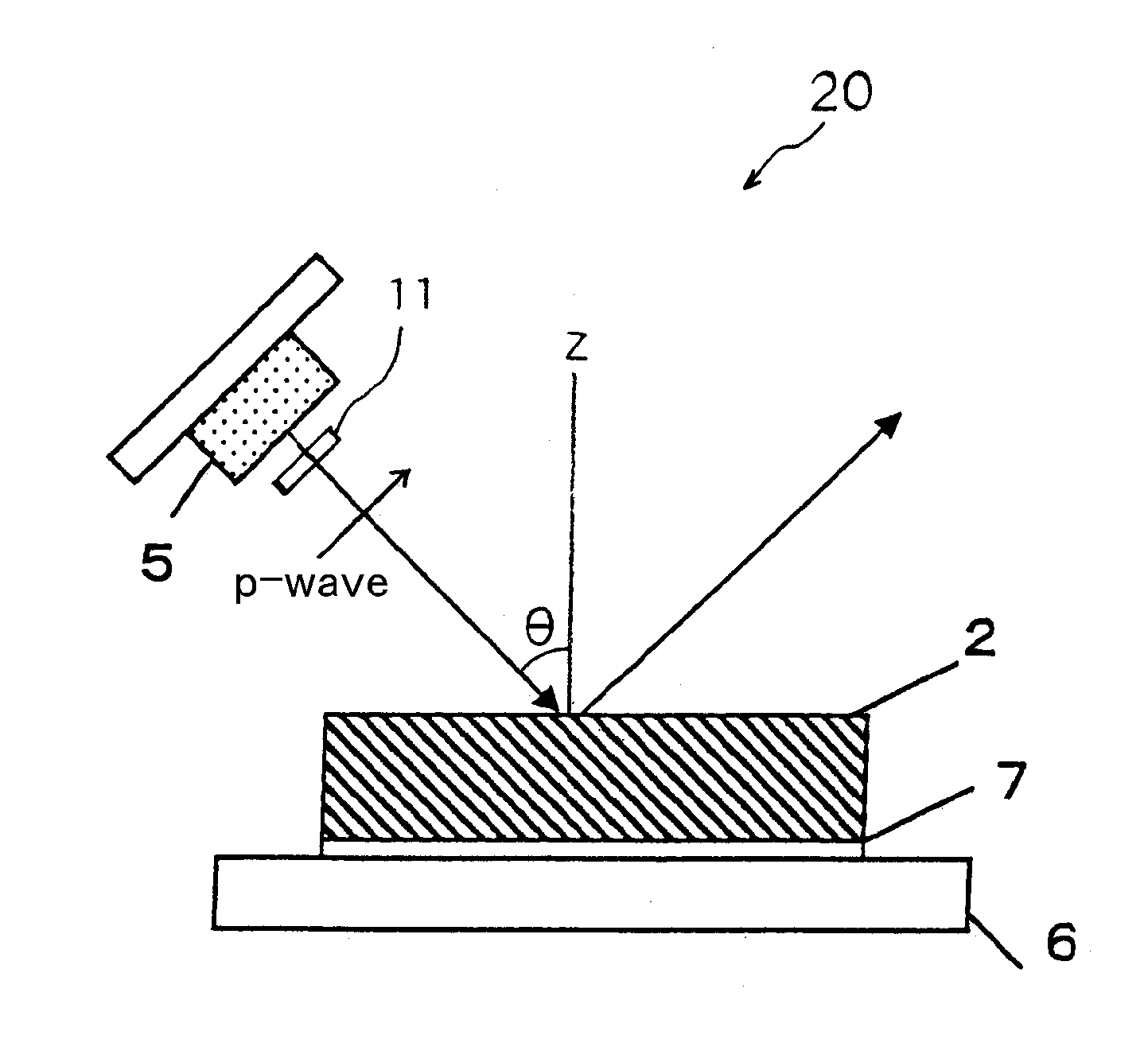
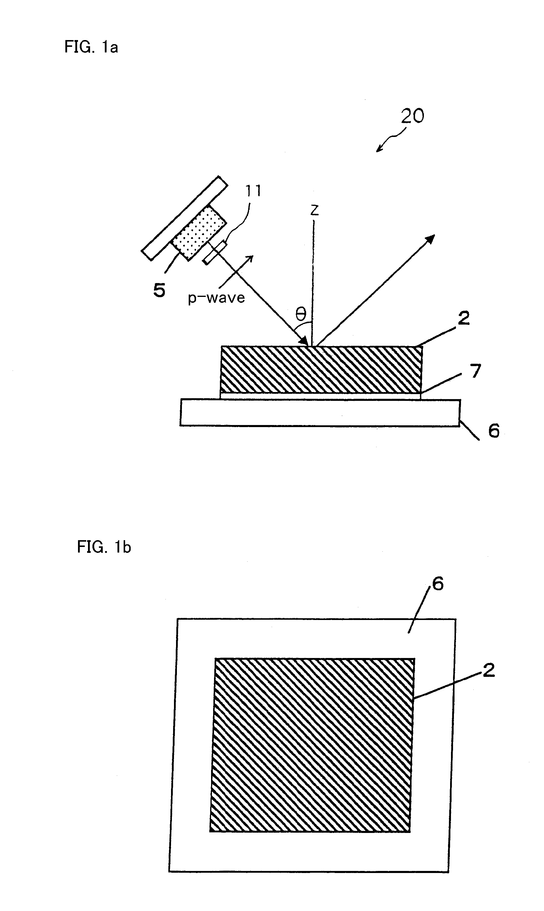
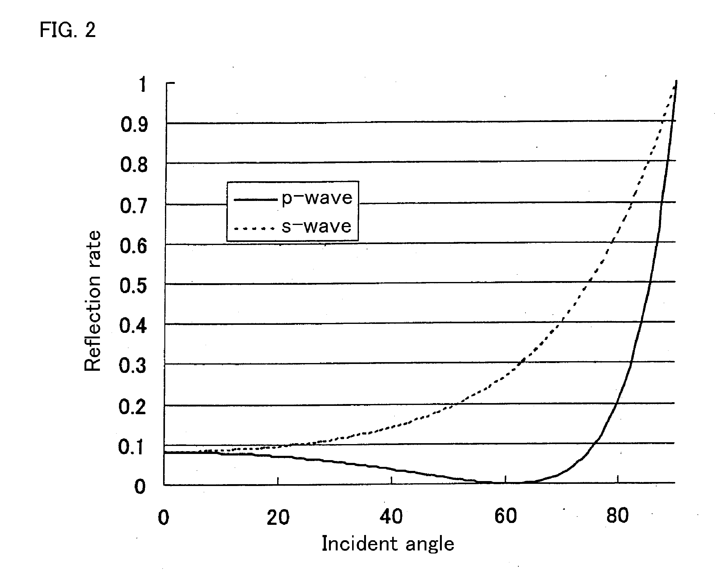
[0047]The disclosed subject matter will now be described in detail with reference to FIGS. 1 to 13, in which the same or corresponding elements use the same reference marks. FIG. 1a is a schematic structural front view showing an exemplary embodiment of a semiconductor light source apparatus made in accordance with principles of the disclosed subject matter, and FIG. 1b is a schematic top view showing a phosphor layer of the embodiment of the semiconductor light source apparatus of FIG. 1a.

[0048]The semiconductor light source apparatus 20 can include a semiconductor light source 5 configured to emit a visible light as excitation light and being an light emitting diode (LED) or a semiconductor laser such as a laser diode, and a phosphor layer 2 including at least one phosphor to wavelength-convert the visible light emitted from the semiconductor light source 5 into an excited light having a longer light-emitting wavelength than that of the light emitted from the semiconductor light ...


PUM


Abstract

A semiconductor light source apparatus can emit various color lights having a substantially uniform color tone and high brightness. The semiconductor light source apparatus can include a radiating substrate, at least one phosphor layer disposed on the radiating substrate and a semiconductor light source emitting blue light. The at least one phosphor layer can be composed of at least one of a glass phosphor and a phosphor ceramic. The light source can be located adjacent the phosphor layer so that the blue light having high brightness can be efficiently reflected on the radiating substrate via the phosphor layer while preventing the blue light from a mirror reflection on the phosphor layer. Thus, the disclosed subject matter can provide a semiconductor light source apparatus that can emit various uniform color lights having high brightness and a lighting unit using the light source apparatus, which can be used for general lighting, vehicle lighting etc.

Description

[0001]This application claims the priority benefit under 35 U.S.C. §119 of Japanese Patent Application No. 2011-052374 filed on Mar. 10, 2011, which is hereby incorporated in its entirety by reference.BACKGROUND[0002]1. Field[0003]The presently disclosed subject matter relates to a semiconductor light source apparatus and a lighting unit using the semiconductor light source apparatus, and more particularly to a high power semiconductor light source apparatus including a phosphor layer that can prevent a reduction of brightness caused by thermal quenching and a lighting unit that can also emit various color lights having a substantially uniform color tone and a large amount of light intensity that can be used for general lighting, such as a stage light, a street light, or a vehicle lamp such as a headlight, etc.[0004]2. Description of the Related Art[0005]Semiconductor light source apparatuses that emit various color lights by combining a phosphor layer with a semiconductor light-emi...

Claims


Application Information

Patent Timeline
Patent Type & Authority Applications(United States)
IPC IPC(8): F21V9/14F21V9/16
CPCF21V9/14F21V9/16C09K11/7774H01L33/507F21S48/1145F21V13/02F21W2131/406F21Y2101/02F21Y2101/025F21K9/00F21Y2115/30F21Y2115/10F21S41/16F21V9/30F21V9/02F21V13/14F21V9/08F21S41/176
Inventor KAWAKAMI, YASUYUKI
Owner STANLEY ELECTRIC CO LTD
Why Eureka
Try Eureka