
Semiconductor light-emitting device and manufacturing method

a technology of semiconductors and light-emitting devices, which is applied in the manufacturing of semiconductor/solid-state devices, semiconductor devices, and electrical devices, etc., can solve the problems of difficulty in reducing the light-emitting surface of the top surface of the encapsulating resin, and the structure including the cavity can achieve the reduction of the light-emitting surface. , the effect of high light-emitting efficiency

Active Publication Date: 2012-09-20
STANLEY ELECTRIC CO LTD
View PDF1 Cites 93 Cited by
  • Summary
  • Abstract
  • Description
  • Claims
  • Application Information

AI Technical Summary

Benefits of technology

[0034]Additionally, the semiconductor light-emitting device can include a reflective material layer having an end of a top surface, disposed between the frame and the side surfaces of the wavelength converting layer and the transparent plate so that the end of the top surface thereof contacts with the side surface of the transparent plate, and the top surface thereof including either one of a concave meniscus shape or a convex meniscus shape, and a light-absorbing layer having an end of a top surface, and disposed on the either one of the concave meniscus shape and the convex meniscus shape of the reflective material layer, wherein the end of the top surface thereof contacts with the side surface of the transparent plate at a higher position than the end of the top surface of the reflective material layer. In this case, a transparent material layer can also located between the transparent plate and the wavelength converting layer so that a side surface thereof is substantially aligned with the side surfaces of the wavelength converting layer and the transparent plate, in order to increase an adhesive strength between the wavelength converting layer and the transparent plate.
[0036]In the above-described exemplary semiconductor light-emitting devices, another reflective material layer can be disposed on the top surface of the light-absorbing layer, and can cover the top surface of the light-absorbing layer in order to prevent the light-absorbing layer from absorbing light emitted from the outside. At least a part of the end of the top surface of the light-absorbing layer can also be located at the substantially edge portion on the side surface of the transparent plate or the wavelength converting layer that becomes a light-emitting surface, to enhance a contrast between the light-emitting surface of the device and a non-light-emitting surface of the light-absorbing layer, which is located adjacent the light-emitting surface.
[0038]According to the above-described exemplary semiconductor light-emitting device, the device can emit a wavelength-converted light having a high light-emitting efficiency and a high contrast between the light-emitting surface and the non-emitting surface from a small light-emitting surface that is slightly larger than the top surface of the light-emitting chip, by utilizing features of the reflective material layer and the light-absorbing layer. Thus, the disclosed subject matter can provide semiconductor light-emitting devices that can emit a wavelength-converted light having a high light-emitting efficiency and a high contrast between the light-emitting surface and the non-emitting surface from the small light-emitting surface, which can be used as a light source for various lighting units.
[0039]Another aspect of the disclosed subject matter includes vehicle headlights using the above-described semiconductor light-emitting device. An exemplary vehicle headlight can include a projector lens having a focus located on an optical axis toward an incident surface, the focus being located at the substantially top surface of the transparent plate, and the incident surface facing the top surface of the transparent plate. Therefore, the disclosed subject matter can provide vehicle headlights using the semiconductor light-emitting device with a simple structure, which can form a light distribution pattern including a horizontal cut-off line having a high contrast by enlarging a light distribution pattern including a light-emitting line having a high contrast emitted from the light-emitting surface of the device using the projector lens.
[0042]According to the exemplary manufacturing method described above for the semiconductor light-emitting devices, the light-absorbing layer used for the light-emitting line having a high contrast can be formed by disposing an uncured light-absorbing material on the either one of the concave meniscus shape or the convex meniscus shape of the reflective material layer. The reflective material layer and the light-absorbing layer can be solidified by a similar method as compared to conventional processes. Thus, the method can provide semiconductor light-emitting devices having a small light-emitting surface, a high contrast between the light-emitting surface and a non-light-emitting surface and a high light-emitting efficiency using manufacturing machines that are similar to those used to manufacture conventional semiconductor light-emitting devices.

Problems solved by technology

Therefore, it may be difficult for a structure including a cavity to reduce a light-emitting surface, because the opening of the cavity becomes the light-emitting surface.
In a structure including the raised encapsulating resin 69 from the base board 62 such as the fourth conventional light source 60, because a relatively large amount of encapsulating resin is required to encapsulate the at least one LED chip 64, the structure may also result in difficulty in reducing the light-emitting surface of the top surface of the encapsulating resin 69.
However, a side surface of the light-shielding layer is exposed to the light-emitting surface, and therefore may absorb a part of light emitted from the LED chips.

Method used


Image

  • Semiconductor light-emitting device and manufacturing method
  • Semiconductor light-emitting device and manufacturing method
  • Semiconductor light-emitting device and manufacturing method

Examples


first embodiment

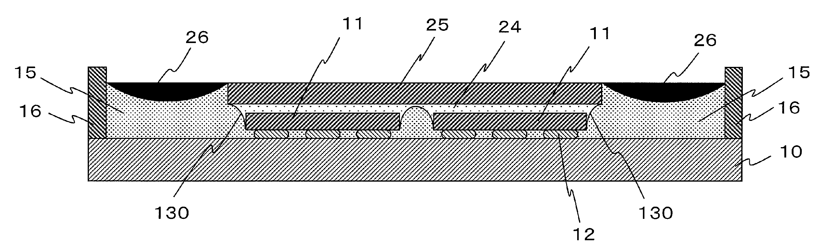
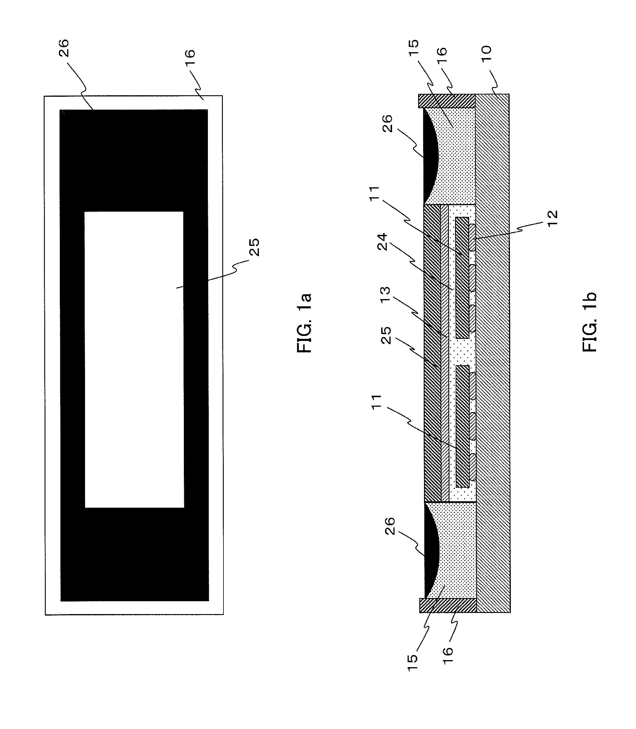
[0117]That is to say, the reflective material layer 15 can perform as a reflector for the semiconductor light-emitting chip 11 by using the side slant surface 130 and the boundary surface contacting with the bottom surface of the semiconductor light-emitting chip 11. Thus, the semiconductor light-emitting device can improve light-emitting efficiency as compared with the conventional device and the device of the

[0118]In addition, because the reflective material layer 15 contacts with the side surface of the wavelength converting layer 14, the top surface of the wavelength converting layer 14 can perform as a light-emitting surface of the semiconductor light-emitting device. Thus, the disclosed subject matter can realize a very small light-emitting surface that is slightly larger than the top surface of the semiconductor light-emitting chip 11, by using the top surface of the wavelength converting layer 14.

[0119]The side slant surface 130 of a boundary between the reflective material ...

second embodiment

[0123] having the above-described structure of the disclosed subject matter, light emitted in an upward direction from the semiconductor light-emitting chip 11 can enter into the wavelength converting layer 14 via the transparent material layer 13, and a wavelength converted light can be emitted from the top surface of the wavelength converting layer 14. Light emitted in a downward direction from the semiconductor light-emitting chip 11 can be reflected at the bottom surface of the light-emitting chip 11 by the reflective material layer 15, and a wavelength converted light can be emitted from the top surface of the wavelength converting layer 14 along with the light emitted in the upward direction from the semiconductor light-emitting chip 11.

[0124]Light emitted in a crosswise direction from the semiconductor light-emitting chip 11 such as light emitted from the side surface of the light-emitting chip 11 can be reflected toward the wavelength converting layer 14 via the transparent ...

third embodiment

[0154]In the first, second and third embodiment, because the top surface of the light-absorbing layer 26 is exposed to the outside of the device, for example when light emitted from the light-emitting device is reflected by a member located outside of the device and enters into the top surface of the light-absorbing layer 26, a temperature of the light-absorbing layer 26 may increase by absorbing the light in the light-absorbing layer 26. Accordingly, a rise in temperature of the light-absorbing layer 26 may cause adverse effect in order for the light-absorbing layer 26 to provide an efficient operation for long periods of time.

[0155]Therefore, the semiconductor light-emitting device can include an other reflective material layer 115, which is disposed on the top surface of the light-absorbing layer 26 disposed in the concave shape of the reflective material layer 15. Thereby, the light-emitting device can prevent the light-absorbing layer 26 from the rise in temperature because the...


PUM


Abstract

A semiconductor light-emitting device and a method for manufacturing the same can include a wavelength converting layer encapsulating at least one semiconductor light-emitting chip to emit various colored lights including white light. The semiconductor light-emitting device can include a base board with the chip mounted thereon, a frame located on the base board, a transparent plate located on the wavelength converting layer, a reflective material layer disposed between the frame and both side surfaces of the wavelength converting layer and the transparent plate, and a light-absorbing layer located on the reflective material layer. The semiconductor light-emitting device can be configured to improve light-emitting efficiency and a contrast between a light-emitting and non-light-emitting surfaces by using the transparent material and light-absorbing layer. A wavelength-converted light that is emitted can have a high light-emitting efficiency and a high contrast between a light-emitting and non-light-emitting surface from a small light-emitting surface.

Description

[0001]This application claims the priority benefit under 35 U.S.C. §119 of Japanese Patent Application No. 2010-201985 filed on Sep. 9, 2010, which is hereby incorporated in its entirety by reference.BACKGROUND[0002]1. Field[0003]The presently disclosed subject matter relates to semiconductor light-emitting devices in which light emitted from a semiconductor light-emitting chip is wavelength-converted by a wavelength converting layer, and to manufacturing methods for the same. More particularly, the disclosed subject matter relates to semiconductor light-emitting devices for a vehicle light and the like, which can form a desired light distribution pattern including a light-emitting line such as a horizontal cut-off line with high light-efficiency, and to methods of manufacturing such devices.[0004]2. Description of the Related Art[0005]Semiconductor light sources, in which a part of the light emitted from a semiconductor light-emitting chip is converted into light having a different...

Claims


Application Information

Patent Timeline
IPC IPC(8): H01L33/60H01L33/52H01L33/08
CPCH01L25/0753H01L33/504H01L33/58H01L33/60H01L2933/005H01L2933/0058H01L2224/48465H01L2224/48091H01L2924/3025H01L2924/00H01L33/56
Inventor SEKO, TOSHIHIROITO, KOSABURO
Owner STANLEY ELECTRIC CO LTD
Features
  • Generate Ideas
  • Intellectual Property
  • Life Sciences
  • Materials
  • Tech Scout
  • Unparalleled Data Quality
  • Higher Quality Content
  • 60% Fewer Hallucinations
Learn More