Two-stage ozone cure for dielectric films

a dielectric film and ozone cure technology, applied in the direction of coatings, metallic material coating processes, chemical vapor deposition coatings, etc., can solve the problems of dielectric material, dielectric material, and structural features of the device having decreased spatial dimensions, so as to reduce or eliminate the effect of increasing the oxygen content of the dielectric layer

Inactive Publication Date: 2012-09-20
APPLIED MATERIALS INC
View PDF18 Cites 122 Cited by
  • Summary
  • Abstract
  • Description
  • Claims
  • Application Information

AI Technical Summary

Benefits of technology

[0006]A method of forming a silicon oxide layer is described. The method increases the oxygen content of a dielectric layer by curing the layer in a two-step ozone cure. The first step involves exposing the dielectric layer to ozone while the second step involves exposing the dielectric layer to ozone excited by a local plasma. This sequence can reduce or eliminate the need for a subsequent anneal following the cure step. The two-step ozone cures may be applied to silicon-and-nitrogen-containing film to convert the films to silicon oxide.

Problems solved by technology

The decreasing feature sizes result in structural features on the device having decreased spatial dimensions.
The widths of gaps and trenches on the device narrow to a point where the aspect ratio of gap depth to its width becomes high enough to make it challenging to fill the gap with dielectric material.
The depositing dielectric material is prone to clog at the top before the gap completely fills, producing a void or seam in the middle of the gap.
However, once these highly flowable materials are deposited, they have to be hardened into a solid dielectric material.
Unfortunately, the departing carbon and hydroxyl species often leave behind pores in the hardened dielectric that reduce the quality of the final material.
In addition, the hardening dielectric also tends to shrink in volume, which can leave cracks and spaces at the interface of the dielectric and the surrounding substrate.

Method used


Image

  • Two-stage ozone cure for dielectric films
  • Two-stage ozone cure for dielectric films
  • Two-stage ozone cure for dielectric films

Examples


Embodiment Construction

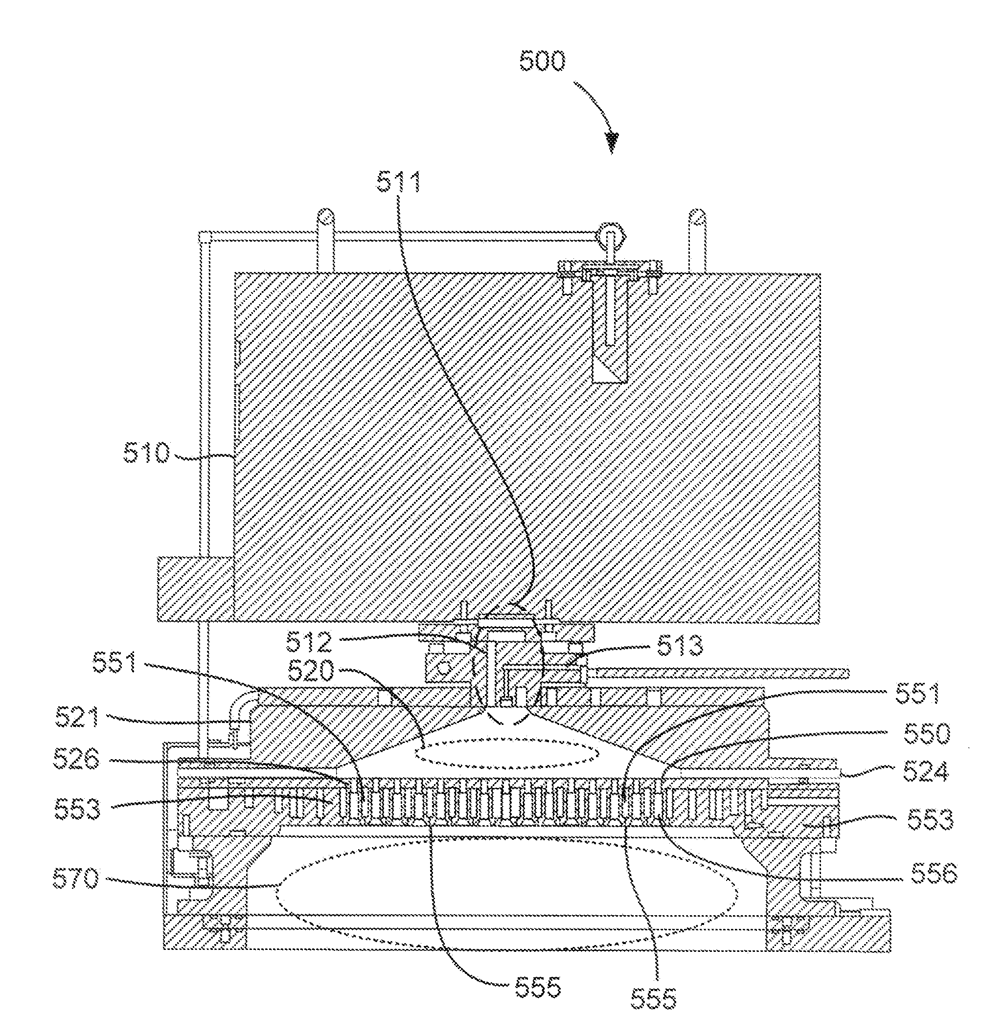
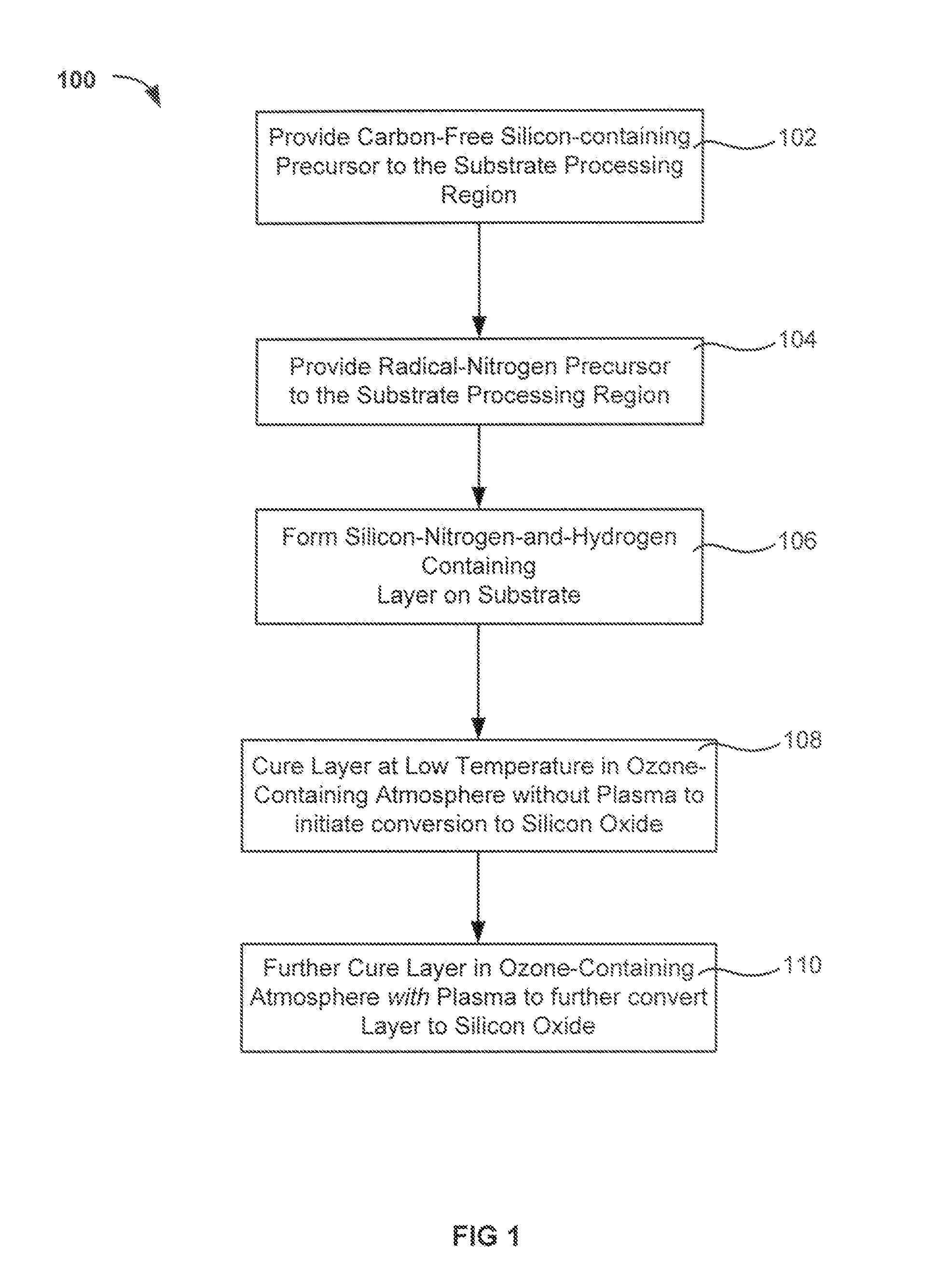
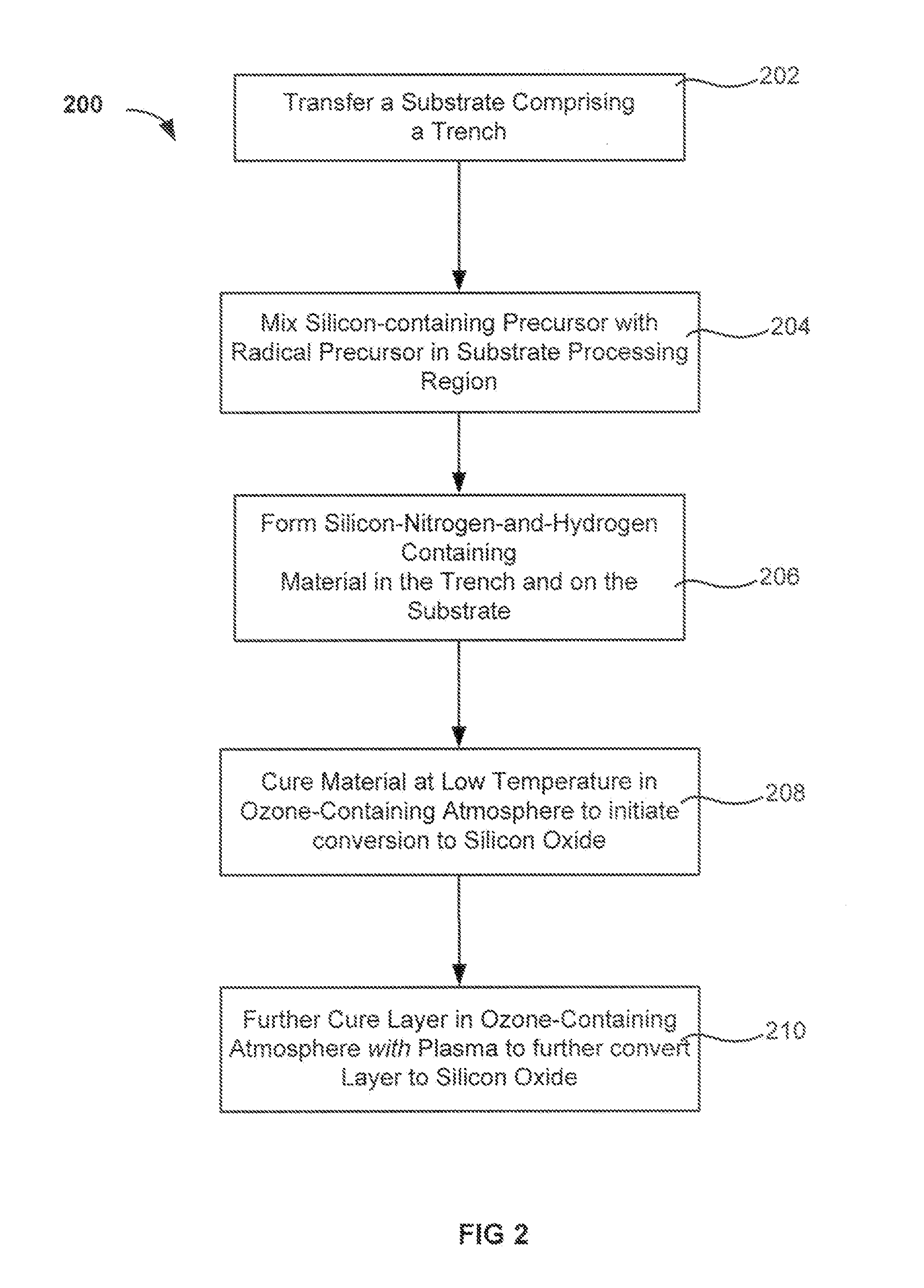
[0016]A method of forming a silicon oxide layer is described. The method increases the oxygen content of a dielectric layer by curing the layer in a two-step ozone cure. The first step involves exposing the dielectric layer to ozone while the second step involves exposing the dielectric layer to ozone excited by a local plasma. This sequence can reduce or eliminate the need for a subsequent anneal following the cure step. The two-step ozone cures may be applied to silicon-and-nitrogen-containing film to convert the films to silicon oxide.

[0017]Without binding the coverage of the claims to hypothetical mechanisms which may or may not be entirely correct, a discussion of some details may prove beneficial. Exposing an as-deposited silicon-and-nitrogen-containing film to ozone first and then exposing it to plasma-excited ozone improves the conversion of the film to silicon oxide over performing either step alone. This may result from the relatively open network produced by depositions o...


PUM

PropertyMeasurementUnit
temperatureaaaaaaaaaa

Abstract

A method of forming a silicon oxide layer is described. The method increases the oxygen content of a dielectric layer by curing the layer in a two-step ozone cure. The first step involves exposing the dielectric layer to ozone while the second step involves exposing the dielectric layer to ozone excited by a local plasma. This sequence can reduce or eliminate the need for a subsequent anneal following the cure step. The two-step ozone cures may be applied to silicon-and-nitrogen-containing film to convert the films to silicon oxide.

Description

CROSS-REFERENCES TO RELATED APPLICATIONS[0001]This application claims the benefit of U.S. Provisional Application No. 61 / 452,362 by Chen et al, filed Mar. 14, 2011 and titled “TWO-STAGE OZONE CURE FOR DIELECTRIC FILMS” which is incorporated herein in its entirety for all purposes.BACKGROUND OF THE INVENTION[0002]Semiconductor device geometries have dramatically decreased in size since their introduction several decades ago. Modern semiconductor fabrication equipment routinely produces devices with 45 nm, 32 nm, and 28 nm feature sizes, and new equipment is being developed and implemented to make devices with even smaller geometries. The decreasing feature sizes result in structural features on the device having decreased spatial dimensions. The widths of gaps and trenches on the device narrow to a point where the aspect ratio of gap depth to its width becomes high enough to make it challenging to fill the gap with dielectric material. The depositing dielectric material is prone to c...

Claims


Application Information

Patent Timeline
Patent Type & Authority Applications(United States)
IPC IPC(8): H01L21/316
CPCC23C16/345C23C16/56H01L21/02164H01L21/31111H01L21/02326H01L21/02337H01L21/0234H01L21/02219
Inventor CHEN, XIAOLINLIANG, JINGMEIINGLE, NITIN K.VENKATARAMAN, SHANKAR
Owner APPLIED MATERIALS INC
Why Eureka
Try Eureka