Pixel circuit of light emitting diode display and driving method thereof

a technology of light-emitting diodes and pixel circuits, which is applied in the direction of instruments, computing, electric digital data processing, etc., can solve the problems of affecting the operation of thin film transistors, affecting the precise control of current isub>oleds/sub>, and the material of oleds certainly ages after the long use time, so as to achieve the effect of increasing the display siz

Inactive Publication Date: 2012-09-27
HANNSTAR DISPLAY CORPORATION
View PDF9 Cites 17 Cited by
  • Summary
  • Abstract
  • Description
  • Claims
  • Application Information

AI Technical Summary

Benefits of technology

[0012]An objective of the present invention is to provide a pixel circuit of a light emitting diode (LED) display and a driving method thereof to totally solve the issues the LED current drop, the luminous efficiency drop and the IR drop due to the larger size of the display.

Problems solved by technology

Comparing with the LCD which merely requires the exact control to the voltage level of the pixel for determining the brightness, the precise control to the current IOLED is much difficult.
Furthermore, the material of the OLED certainly ages after the long usage time.
The increase of the OLED voltage also can affect the operation of the thin film transistor.
Furthermore, the luminous efficiency of the OLED drops because the material of the OLED certainly ages after the long usage time.
Due to the luminous efficiency drop, even the same current flowing through the OLED, the expected brightness cannot be realized.
Besides, the luminous efficiency drops of the tricolor are different and more serious issue of the color cast occurs.
Moreover, with the size of the display becomes larger, an IR drop issue occurs.

Method used


Image

  • Pixel circuit of light emitting diode display and driving method thereof
  • Pixel circuit of light emitting diode display and driving method thereof
  • Pixel circuit of light emitting diode display and driving method thereof

Examples


first embodiment

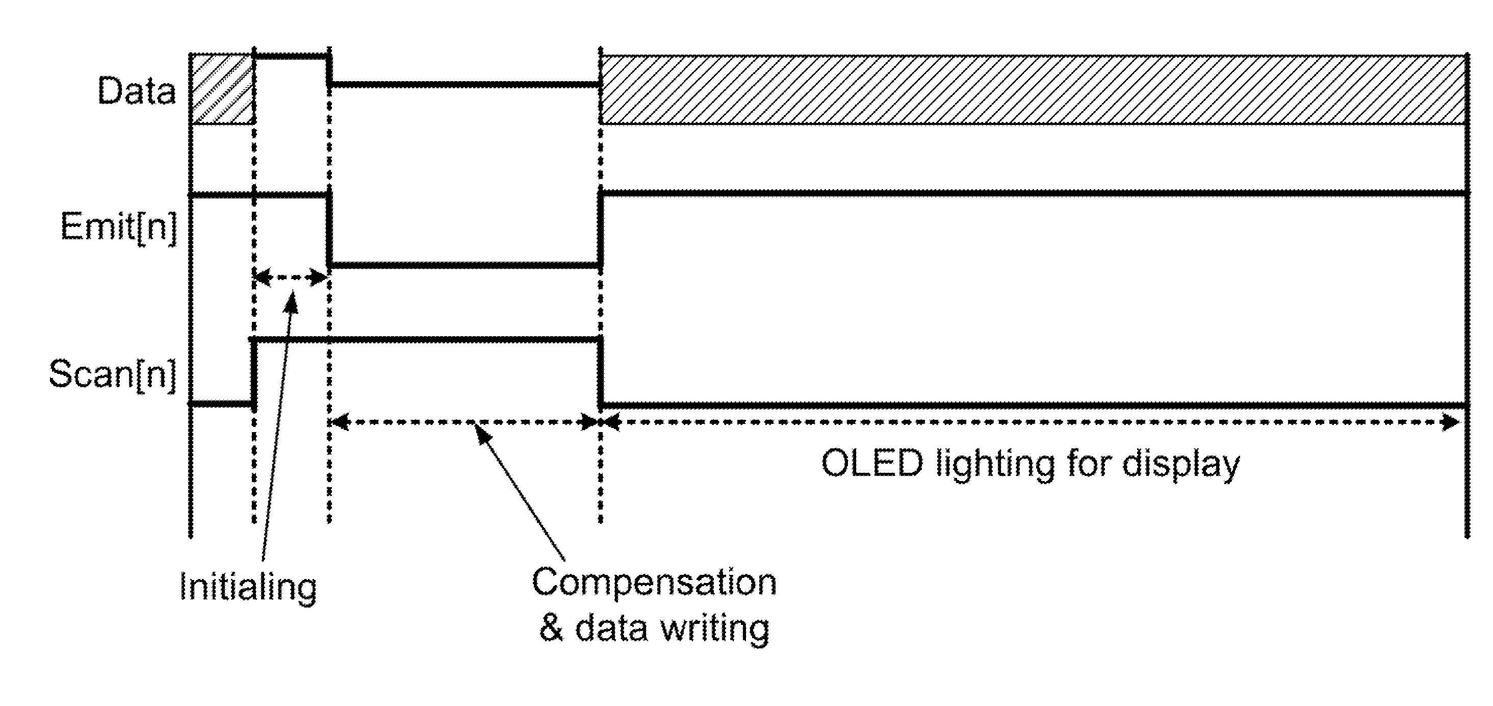
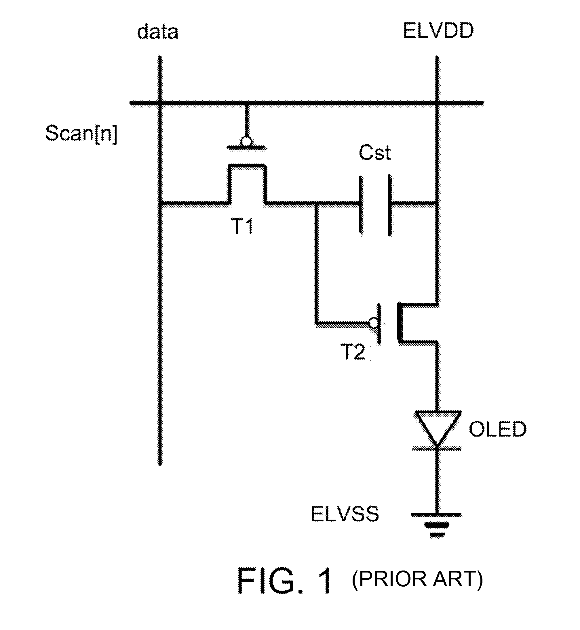
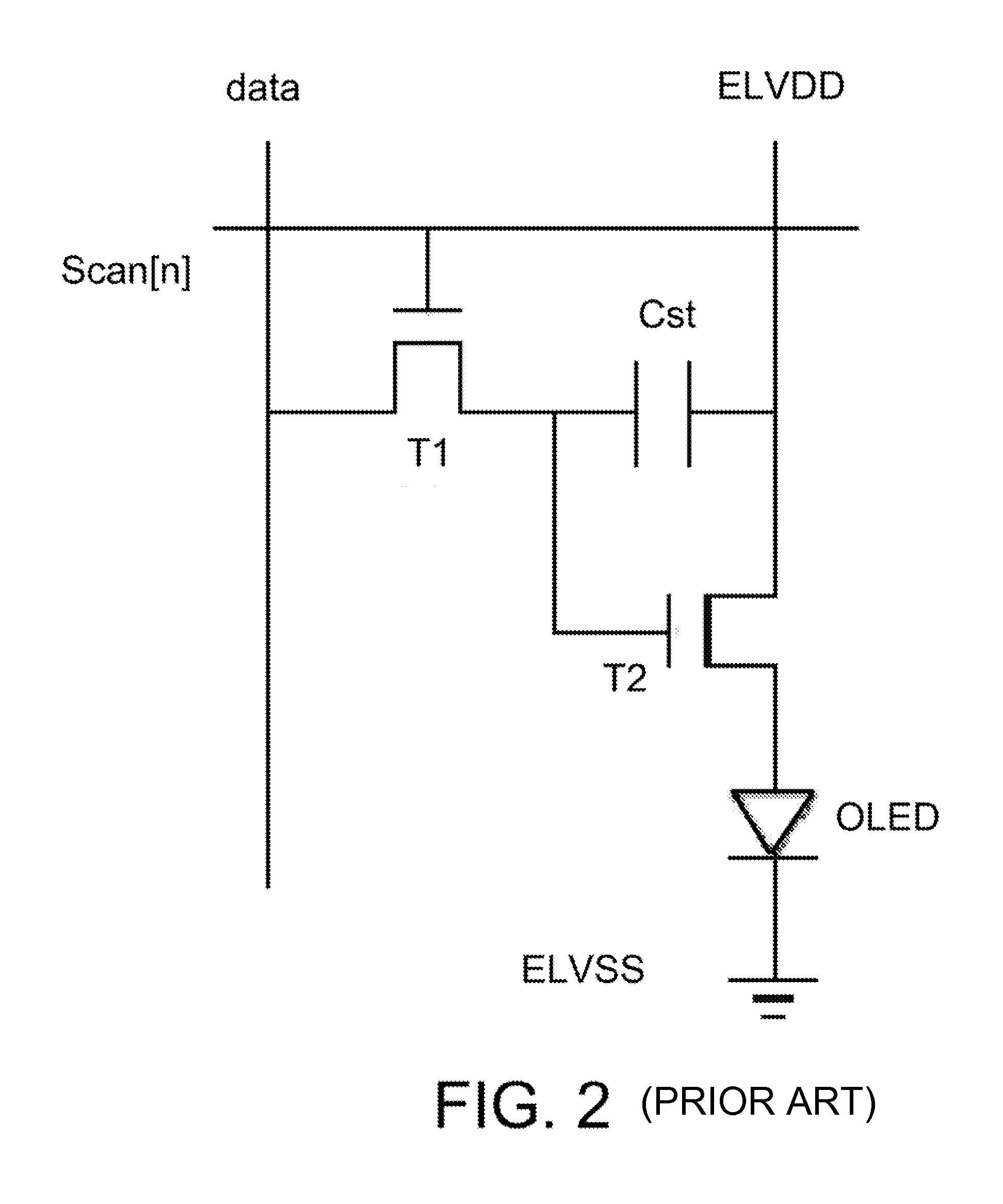
[0029]Please refer to FIG. 4, which depicts a diagram of a pixel circuit of an active matrix organic light emitting diode (AMOLED) display according to the present invention. As shown in figures, the first thin film transistor is an N type thin film transistor. The second, third, fourth and fifth thin film transistors are P type thin film transistors. Meanwhile, the present invention does not need a storage capacitance Cst as in prior art. The light emitting diode display shown in FIG. 4 has a data line (Data), an emit line (Emit[n]) and a scan line (Scan[n]) coupled to the pixel circuit. The variable n represents the pixel is one among lots of pixels of the display. The light emitting diode display provides an operating voltage VDD and a grounding voltage VSS to the pixel circuit. The pixel circuit of the light emitting diode display comprises a first thin film transistor T1, an organic light emitting diode OLED, a second thin film transistor T2, a third thin film transistor T3, a ...

second embodiment

[0044]Please refer to FIG. 7, which depicts a diagram of a pixel circuit of an active matrix organic light emitting diode (AMOLED) display according to the present invention. As shown in figures, the first thin film transistor is a P type thin film transistor. The second, third, fourth and fifth thin film transistors are N type thin film transistors. Meanwhile, the present invention does not need a storage capacitance Cst as in prior art. The light emitting diode display shown in FIG. 7 has a data line (Data), an emit line (Emit[n]) and a scan line (Scan[n]) coupled to the pixel circuit. The variable n represents the pixel is one among lots of pixels of the display. The light emitting diode display provides an operating voltage VDD and a grounding voltage VSS to the pixel circuit. The pixel circuit of the light emitting diode display comprises a first thin film transistor T1, an organic light emitting diode OLED, a second thin film transistor T2, a third thin film transistor T3, a f...


PUM


Abstract

The gate of the first TFT in the present invention is discharged through the first TFT and the OLED in the compensation and data writing stage operation. As in cases that the usage time of the display pixel extends and the threshold voltage of the first TFT increases and the mobility thereof decreases, the voltage of the OLED increases, or the size of the display becomes larger to induce IR drop, the present invention enables to reduce the discharge voltage (charge current) to raise the gate voltage of the first TFT for compensating the OLED current drop. Meanwhile, the fifth TFT has characteristic of the threshold voltage increase. As the threshold voltage of the fifth TFT increases with usage time, the compensation of the OLED luminous efficiency drop can be realized.

Description

BACKGROUND OF THE INVENTION[0001]1. Field of the Invention[0002]The present invention generally relates to a pixel circuit of a light emitting diode display, and more particularly to a pixel circuit of a light emitting diode (LED) display and a driving method thereof for totally solving issues of LED current drop, luminous efficiency drop and IR drop due to the larger size of the display.[0003]2. Description of Prior Art[0004]The LCD is the mainstream of display technology. However, the OLED display is considered to replace the LCD by related industry and is going to be the next generation display. Comparing with the LCD, the OLED display possesses tons of advantages. For example, self lighting, wide view angle, rapid response time, high brightness, high luminous efficiency, low operating voltage, thin panel, flexibility, few processes, low cost and et cetera.[0005]However, the biggest difference between the OLED and the LCD is that the brightness of the OLED is determined by the cu...

Claims


Application Information

Patent Timeline
Patent Type & Authority Applications(United States)
IPC IPC(8): G09G3/32G09G5/10G09G5/00
CPCG09G3/3233G09G2320/045G09G2300/0861G09G3/3291G09G2320/0223
Inventor KO, CHIEN-CHUANWU, CHAO-HUI
Owner HANNSTAR DISPLAY CORPORATION
Why Eureka
Try Eureka