Semiconductor Device

a technology of semiconductor devices and semiconductors, applied in the direction of semiconductor devices, photovoltaic energy generation, electrical apparatus, etc., can solve the problems of parasitic capacitance between, increase in resolution, etc., and achieve the effect of increasing the screen size of a display device, low manufacturing cost, and relatively simple manufacturing process

Active Publication Date: 2017-01-26
SEMICON ENERGY LAB CO LTD
View PDF23 Cites 27 Cited by
  • Summary
  • Abstract
  • Description
  • Claims
  • Application Information

AI Technical Summary

Benefits of technology

[0012]As examples of a transistor including an oxide semiconductor film, an inverted staggered transistor (also referred to as a bottom-gate transistor) and a staggered transistor (also referred to as a top-gate transistor) can be given. In the case where a transistor including an oxide semiconductor film is used for a display device, an inverted staggered transistor is used more often than a staggered transistor because its manufacturing process is relatively simple and its manufacturing cost is low. However, an increase in the screen size of a display device or an increase in the resolution of an image on a display device (e.g., a high-resolution display device typified by a 4K×2K display device (3840 pixels in the horizontal direction and 2160 pixels in the vertical direction) or an 8K×4K display device (7680 pixels in the horizontal direction and 4320 pixels in the vertical direction)) might cause parasitic capacitance between a gate electrode and source and drain electrodes in an inverted staggered transistor. Depending on the value of the parasitic capacitance, a signal delay or the like becomes more severe, leading to degradation of the display quality of the display device. Thus, regarding a staggered transistor including an oxide semiconductor film, a structure with stable semiconductor characteristics and high reliability is desired to be developed.

Problems solved by technology

However, an increase in the screen size of a display device or an increase in the resolution of an image on a display device (e.g., a high-resolution display device typified by a 4K×2K display device (3840 pixels in the horizontal direction and 2160 pixels in the vertical direction) or an 8K×4K display device (7680 pixels in the horizontal direction and 4320 pixels in the vertical direction)) might cause parasitic capacitance between a gate electrode and source and drain electrodes in an inverted staggered transistor.
Depending on the value of the parasitic capacitance, a signal delay or the like becomes more severe, leading to degradation of the display quality of the display device.
Furthermore, in the case where a transistor is formed using an oxide semiconductor film for a channel region, an oxygen vacancy which is formed in the channel region of the oxide semiconductor film adversely affects the transistor characteristics.
Furthermore, there is a problem in that electrical characteristics vary among transistors.

Method used


Image

  • Semiconductor Device
  • Semiconductor Device
  • Semiconductor Device

Examples


embodiment 1

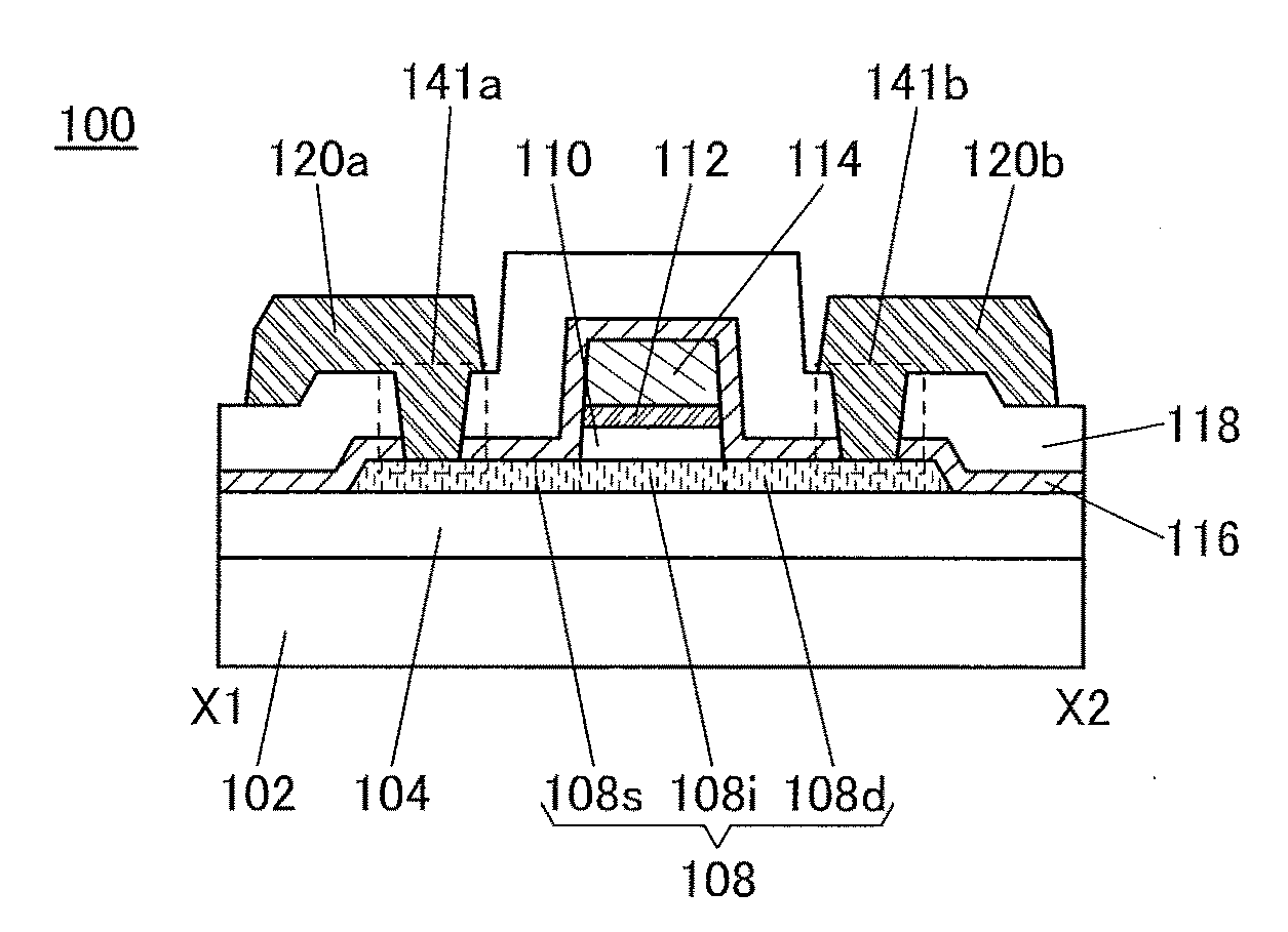
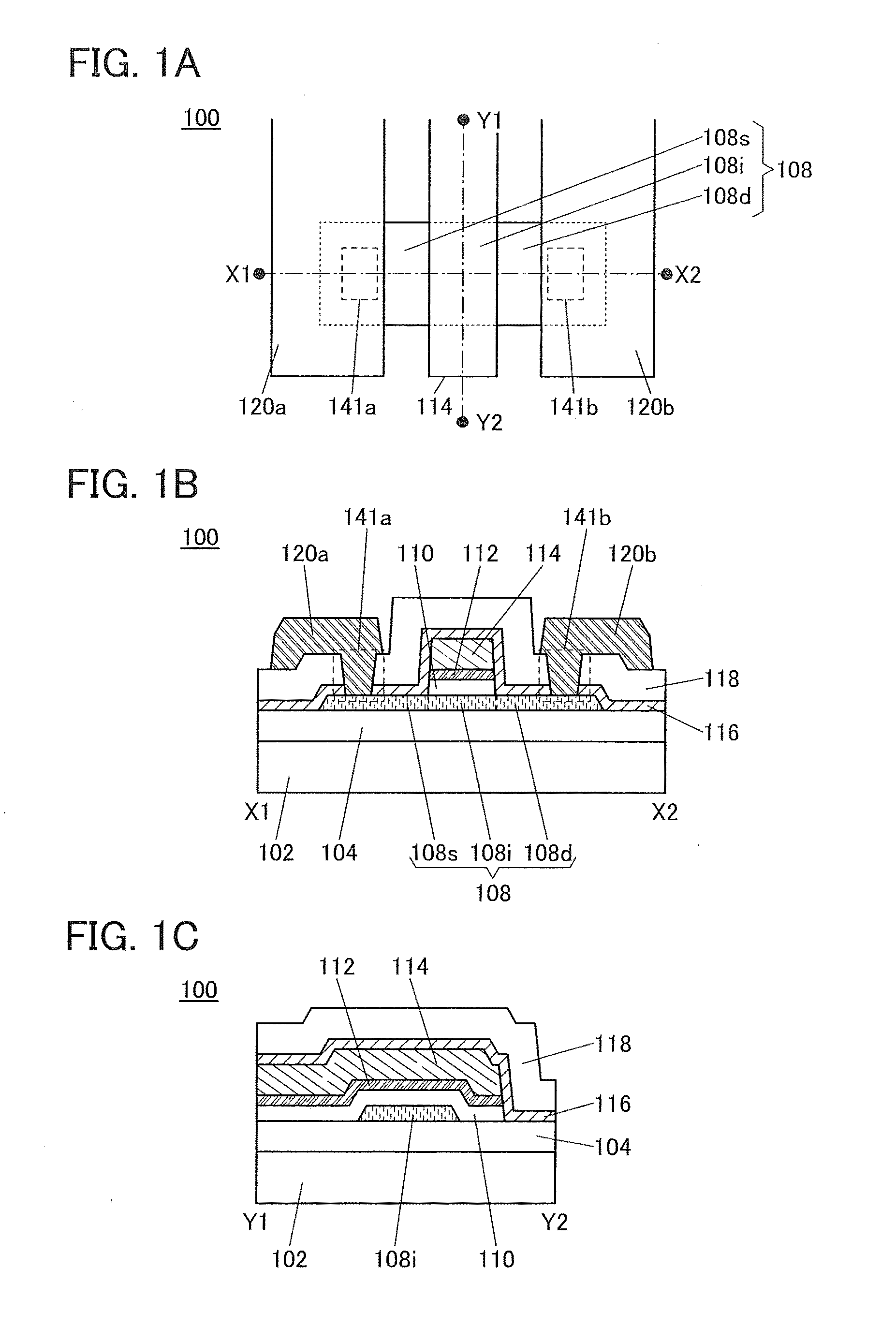
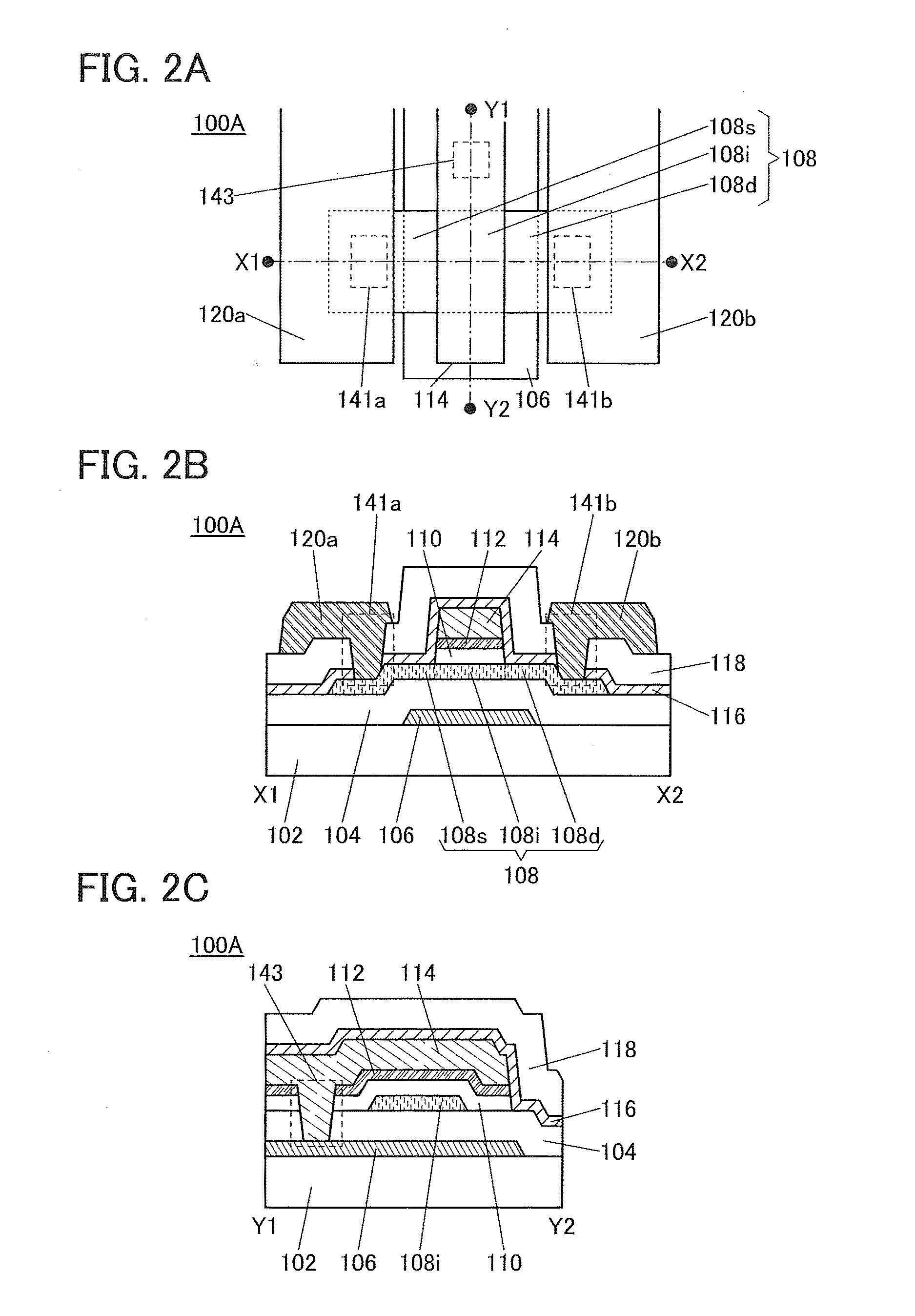
[0105]In this embodiment, examples of a semiconductor device including a transistor and a method for manufacturing the semiconductor device will be described with reference to FIGS. 1A to 1C through FIGS. 20A to 20D.

[0106]FIGS. 1A to 1C illustrate an example of a semiconductor device including a transistor. Note that the transistor in FIGS. 1A to 1C has a staggered (top-gate) structure.

[0107]FIG. 1A is a top view of a transistor 100. FIG. 1B is a cross-sectional view taken along dashed-dotted line X1-X2 in FIG. 1A. FIG. 1C is a cross-sectional view taken along dashed-dotted line Y1-Y2 in FIG. 1A. For clarity, FIG. 1A does not illustrate some components such as an insulating film 110. As in FIG. 1A, some components are not illustrated in some cases in top views of transistors described below. Furthermore, the direction of dashed-dotted line X1-X2 may be referred to as a channel length (L) direction, and the direction of dashed-dotted line Y1-Y2 may be referred to as a channel width (...

embodiment 2

[0314]In this embodiment, an oxygen vacancy (VO) formed in an oxide semiconductor and the case where an impurity (fluorine or hydrogen) enters the oxygen vacancy are described in detail.

O) Formed in Oxide Semiconductor>

[0315]First, a model of an oxygen vacancy (VO) formed in an oxide semiconductor is described. In an oxide semiconductor, an oxygen vacancy forms a deep level (also referred to as dDOS). The dDOS degrades the electrical characteristics of a transistor including an oxide semiconductor in some cases. Described here are the results of examining a model where a cluster of oxygen vacancies (also referred to as a VO cluster) is formed in an oxide semiconductor.

[0316]FIG. 21A illustrates an InGaZnO4 crystal model in an initial state (before an oxygen vacancy is formed). FIGS. 21B and 21C and FIGS. 22A to 22C illustrate a model where oxygen vacancies are formed in the InGaZnO4 crystal model in the initial state shown in FIG. 21A. In FIGS. 21A to 21C and FIGS. 22A to 22C, a whi...

embodiment 3

[0393]In this embodiment, the structure and the like of an oxide semiconductor will be described with reference to FIGS. 37A to 37E, FIGS. 38A to 38E, FIGS. 39A to 39D, FIGS. 40A and 40B, and FIG. 41.

[0394]An oxide semiconductor is classified into a single-crystal oxide semiconductor and a non-single-crystal oxide semiconductor. Examples of the non-single-crystal oxide semiconductor include a c-axis aligned crystalline oxide semiconductor (CAAC-OS), a polycrystalline oxide semiconductor, a nanocrystalline oxide semiconductor (nc-OS), an amorphous-like oxide semiconductor (a-like OS), and an amorphous oxide semiconductor.

[0395]From another perspective, an oxide semiconductor is classified into an amorphous oxide semiconductor and a crystalline oxide semiconductor. Examples of the crystalline oxide semiconductor include a single-crystal oxide semiconductor, a CAAC-OS, a polycrystalline oxide semiconductor, and an nc-OS.

[0396]An amorphous structure is generally thought to be isotropic ...


PUM


Abstract

In a transistor including an oxide semiconductor, a change in electrical characteristics is suppressed and reliability is improved. The transistor includes an oxide semiconductor film over a first insulating film; a second insulating film over the oxide semiconductor film; a metal oxide film over the second insulating film; a gate electrode over the metal oxide film; and a third insulating film over the oxide semiconductor film and the gate electrode. The oxide semiconductor film includes a channel region overlapping with the gate electrode, a source region in contact with the third insulating film, and a drain region in contact with the third insulating film. The source region and the drain region contain one or more of hydrogen, boron, carbon, nitrogen, fluorine, phosphorus, sulfur, chlorine, titanium, and a rare gas.

Description

BACKGROUND OF THE INVENTION[0001]1. Field of the Invention[0002]One embodiment of the present invention relates to a semiconductor device including an oxide semiconductor film and a display device including the semiconductor device.[0003]Note that one embodiment of the present invention is not limited to the above technical field. The technical field of one embodiment of the invention disclosed in this specification and the like relates to an object, a method, or a manufacturing method. In addition, the present invention relates to a process, a machine, manufacture, or a composition of matter. In particular, one embodiment of the present invention relates to a semiconductor device, a display device, a light-emitting device, a power storage device, a memory device, a driving method thereof, or a manufacturing method thereof.[0004]In this specification and the like, a semiconductor device generally means a device that can function by utilizing semiconductor characteristics. A semicond...

Claims


Application Information

Patent Timeline
Patent Type & Authority Applications(United States)
IPC IPC(8): H01L29/786H01L29/66H01L27/12H01L29/24H01L29/04
CPCH01L29/78606H01L29/7869H01L29/78696H01L29/66969H01L29/24H01L29/045H01L27/1225H01L29/78618H01L29/41733H01L29/4908H01L29/78648Y02E10/549H01L29/786H01L29/7849
Inventor YAMAZAKI, SHUNPEIOKAZAKI, KENICHIKOEZUKA, JUNICHINAKAYAMA, TOMONORINAKASHIMA, MOTOKI
Owner SEMICON ENERGY LAB CO LTD
Why Eureka
Try Eureka