Array substrate and display device

A technology of array substrates and common electrodes, applied in optics, instruments, electrical components, etc., can solve problems affecting panel resolution, loss, large aperture ratio, etc., and achieve the effects of avoiding display quality problems, power reduction, and high aperture ratio

Active Publication Date: 2013-03-13
BOE TECH GRP CO LTD
View PDF6 Cites 11 Cited by
  • Summary
  • Abstract
  • Description
  • Claims
  • Application Information

AI Technical Summary

Problems solved by technology

As the size of the panel increases and the resolution increases, the pixel area becomes smaller and smaller. Such a structure will cause a large loss of aperture ratio and affect the resolution of the panel.

Method used


Image

  • Array substrate and display device
  • Array substrate and display device
  • Array substrate and display device

Examples


Embodiment Construction

[0029] The array substrate and the display device proposed by the present invention are described in detail below with reference to the drawings and embodiments.

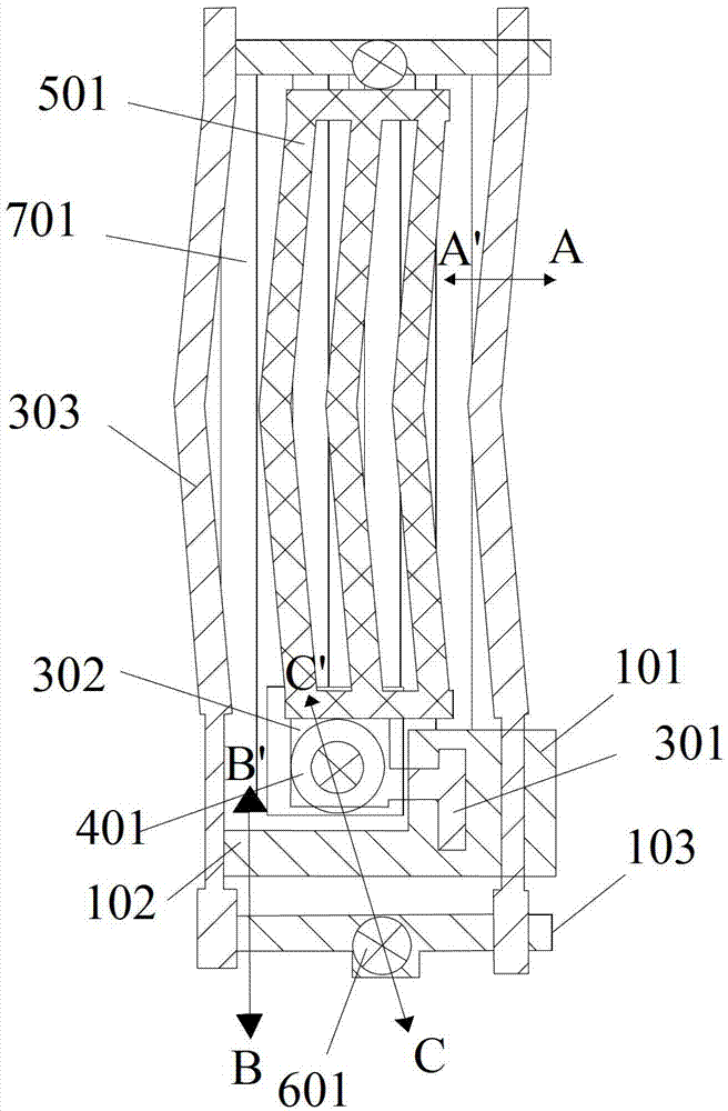
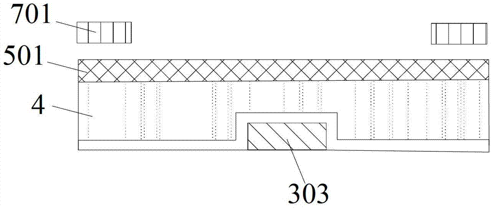
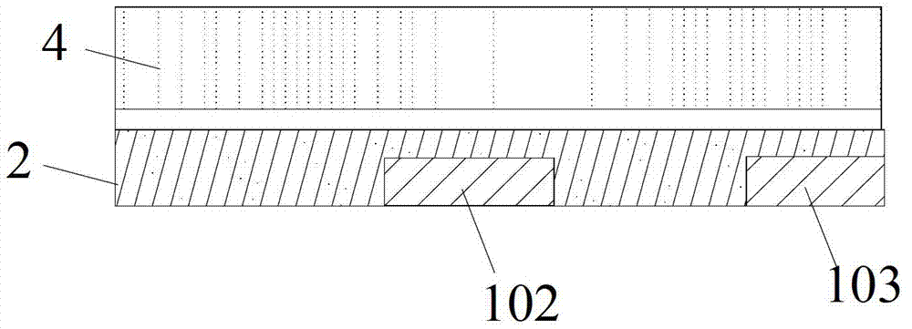
[0030] Such as Figure 5~7 As shown, an array substrate according to an embodiment of the present invention includes: a plurality of gate lines 102 , data lines 303 formed on the substrate, and a plurality of pixel units defined between the gate lines 102 and the data lines 303 . It also includes a common electrode line (not shown in the figure) connected to the common electrode. The pixel unit also includes: a thin film transistor, a pixel electrode 701 and a common electrode 501 . The gate 101 of the TFT is formed in the same layer as the gate line 102 , the source 301 is connected to the data line 303 , and the drain 302 is connected to the pixel electrode 701 through a via hole (not shown in the figure). The data line 303 does not overlap with the common electrode, that is, the projection of the data line 303 ...


PUM


Abstract

The invention discloses an array substrate, and relates to the technical field of display. The array substrate comprises a plurality of grid lines, data lines and a plurality of pixel units defined by the crossing of the grid lines and the data lines. Each pixel unit comprises a thin film transistor, a pixel electrode and a common electrode. The data lines are not overlapped with the common electrodes. The invention also discloses a display device comprising the array substrate. According to the array substrate, the problems of poor correlation and low power consumption caused by the coupling of the data lines and the common electrodes are solved, and a higher aperture ratio and higher resolution can also be ensured.

Description

technical field [0001] The present invention relates to the field of display technology, in particular to an array substrate and a display device. Background technique [0002] Advanced Super Dimension Switch technology (ADvanced Super Dimension Switch, ADS) is the core technology of planar electric field wide viewing angle. The multi-dimensional electric field makes all oriented liquid crystal molecules between the slit electrodes in the liquid crystal cell and directly above the electrodes rotate. Therefore, the working efficiency of the liquid crystal is improved and the light transmission efficiency is increased. Advanced ultra-dimensional field conversion technology can improve the picture quality of TFT-LCD products, with high resolution, high transmittance, low power consumption, wide viewing angle, high aperture ratio, low color difference, no push Mura, etc. advantage. [0003] At present, ADS panels are widely used, and its improved technology also includes ADS ...

Claims


Application Information

Patent Timeline
Patent Type & Authority Applications(China)
IPC IPC(8): G02F1/1362G02F1/1368G02F1/1343
CPCG02F1/136286G02F2001/134318G02F2001/134372G02F2001/13606G02F1/134363G02F1/134318G02F1/13606G02F1/134372H01L27/124H01L27/156
Inventor 严允晟崔贤植徐智强李会
Owner BOE TECH GRP CO LTD
Why Eureka
Try Eureka