Configuration and method to generate saddle junction electric field in edge termination

Active Publication Date: 2012-10-04
ALPHA & OMEGA SEMICON INC
View PDF9 Cites 39 Cited by
  • Summary
  • Abstract
  • Description
  • Claims
  • Application Information

AI Technical Summary

Benefits of technology

[0008]It is therefore an aspect of the present invention to provide a new and improved edge termination configuration to reduce the electrical field crowding effects near the blocking junction at the device edge and provide a compact termination with lower surface el

Problems solved by technology

Conventional manufacturing technologies and device configuration to further increase the breakdown voltage of a semiconductor power device at the terminal areas are still confronted with difficulties that the termination areas occupied large areas.
The difficulties are becoming even more severe and limiting when the semiconductor power devices are now manufactured with ever reduced size.
However, as size of the chip becomes smaller and smaller, the percentage of the edge termination gradually increases and may take up to about 50% of the total area in order to maintain a high breakdown voltage.
The termination area is a “non-active” area of a transistor because it is not useful for current conduction.
Even though

Method used


Image

  • Configuration and method to generate saddle junction electric field in edge termination
  • Configuration and method to generate saddle junction electric field in edge termination
  • Configuration and method to generate saddle junction electric field in edge termination

Examples


Embodiment Construction

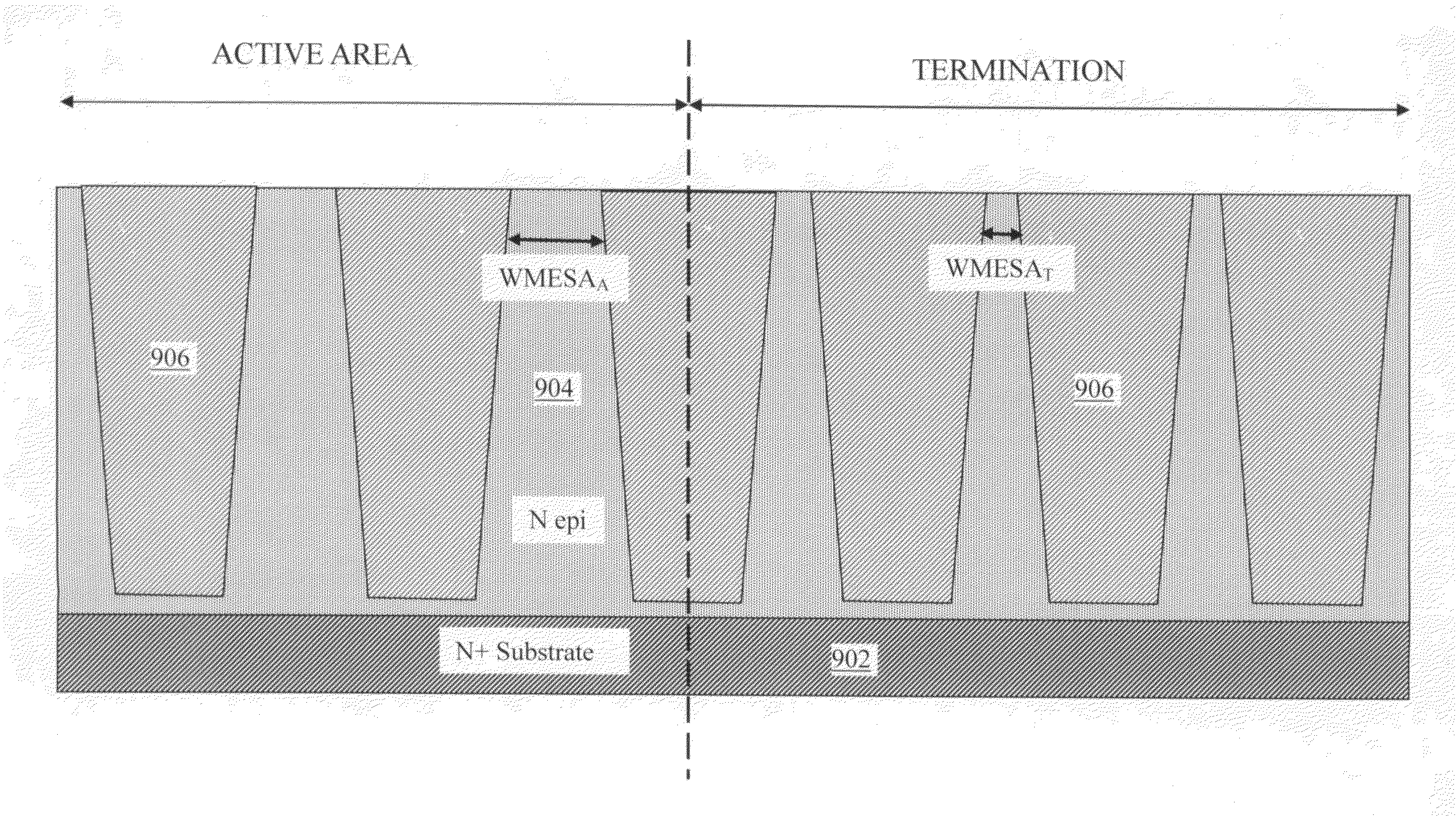
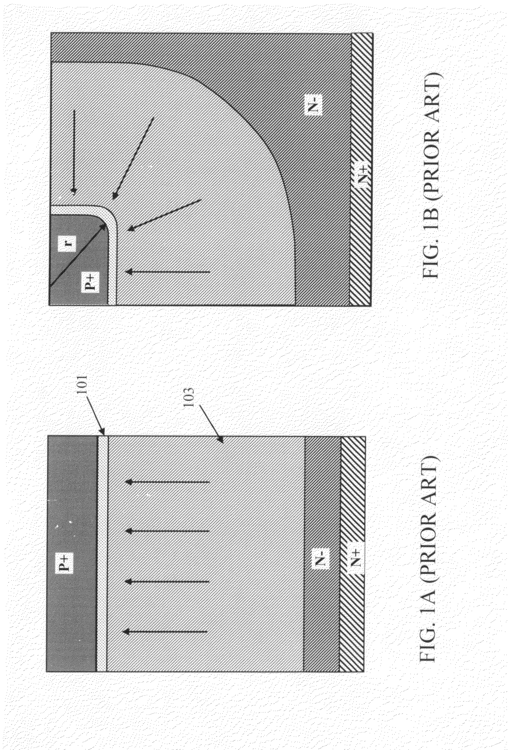
[0025]For better understanding the invention, FIG. 2 is described as an edge termination configuration with a saddle junction configuration. By definition, a junction is created when a P region diffuse into N type semiconductor region. The saddle junction has the opposite curvature to that of a cylindrical junction, which ameliorates the electric filed crowding and increase the breakdown voltage. Compare to the cylindrical junction shown in FIG. 1B, the lightly doped N type region is replaced with a lightly doped P type region 107 and a junction is formed between the lightly doped P type region 107 and a heavy doped N type edge region 104 and substrate 105 surrounding the lightly doped P type region 107 having a depletion region 106. A heavily doped P+ region 115 is provided for the prevention of reach through breakdown. This saddle junction configuration shifts the peak electric field down to the N+ substrate, and generates a negative charge concave junction that spread out the ele...


PUM


Abstract

This invention discloses a semiconductor power device disposed in a semiconductor substrate and having an active cell area and an edge termination area the edge termination area wherein the edge termination area comprises a superjunction structure having doped semiconductor columns of alternating conductivity types with a charge imbalance between the doped semiconductor columns to generate a saddle junction electric field in the edge termination.

Description

BACKGROUND OF THE INVENTION[0001]1. Field of the Invention[0002]The invention relates generally to the semiconductor power devices. More particularly, this invention relates to configurations and methods for manufacturing of new and improved edge terminations for semiconductor power devices to generate electrical field as saddle junctions to reduce the areas occupied by the termination areas while maintaining high breakdown voltages.[0003]2. Description of the Prior Art[0004]Conventional manufacturing technologies and device configuration to further increase the breakdown voltage of a semiconductor power device at the terminal areas are still confronted with difficulties that the termination areas occupied large areas. The difficulties are becoming even more severe and limiting when the semiconductor power devices are now manufactured with ever reduced size. A general survey discovers that for integrate circuit (IC) chips of larger size; the edge termination takes up about 20% of th...

Claims


Application Information

Patent Timeline
IPC IPC(8): H01L29/06H01L21/20
CPCH01L29/0615H01L29/861H01L29/6609H01L29/0634H01L21/26513H01L21/761H01L29/0619
Inventor BOBDE, MADHURGUAN, LINGPENGBHALLA, ANUPYILMAZ, HAMZA
Owner ALPHA & OMEGA SEMICON INC
Why Eureka
Try Eureka