Semiconductor device and method of manufacturing the same

a technology of semiconductor devices and semiconductors, applied in semiconductor devices, semiconductor/solid-state device details, electrical apparatus, etc., to achieve the effect of preventing cracks

Inactive Publication Date: 2012-10-04
ABLIC INC
View PDF2 Cites 16 Cited by
  • Summary
  • Abstract
  • Description
  • Claims
  • Application Information

AI Technical Summary

Benefits of technology

[0009]According to the present invention, the stress generated by the impact of wire-bonding is mostly absorbed in the porous metal film owing to the distortion of the porous metal film. Accordingly, it is possible to prevent the generation of the cracks in the insulating film provided under the porous metal film due to the stress generated by this impact.

Problems solved by technology

However there has been a risk that in a conventional semiconductor device having a pad, due to the stress generated by the impact of wire-bonding, cracks might be found in the pad made of the metal film 92 or in the insulating film 91 under the pad, which has also been a problem.

Method used


Image

  • Semiconductor device and method of manufacturing the same
  • Semiconductor device and method of manufacturing the same
  • Semiconductor device and method of manufacturing the same

Examples


modification 9

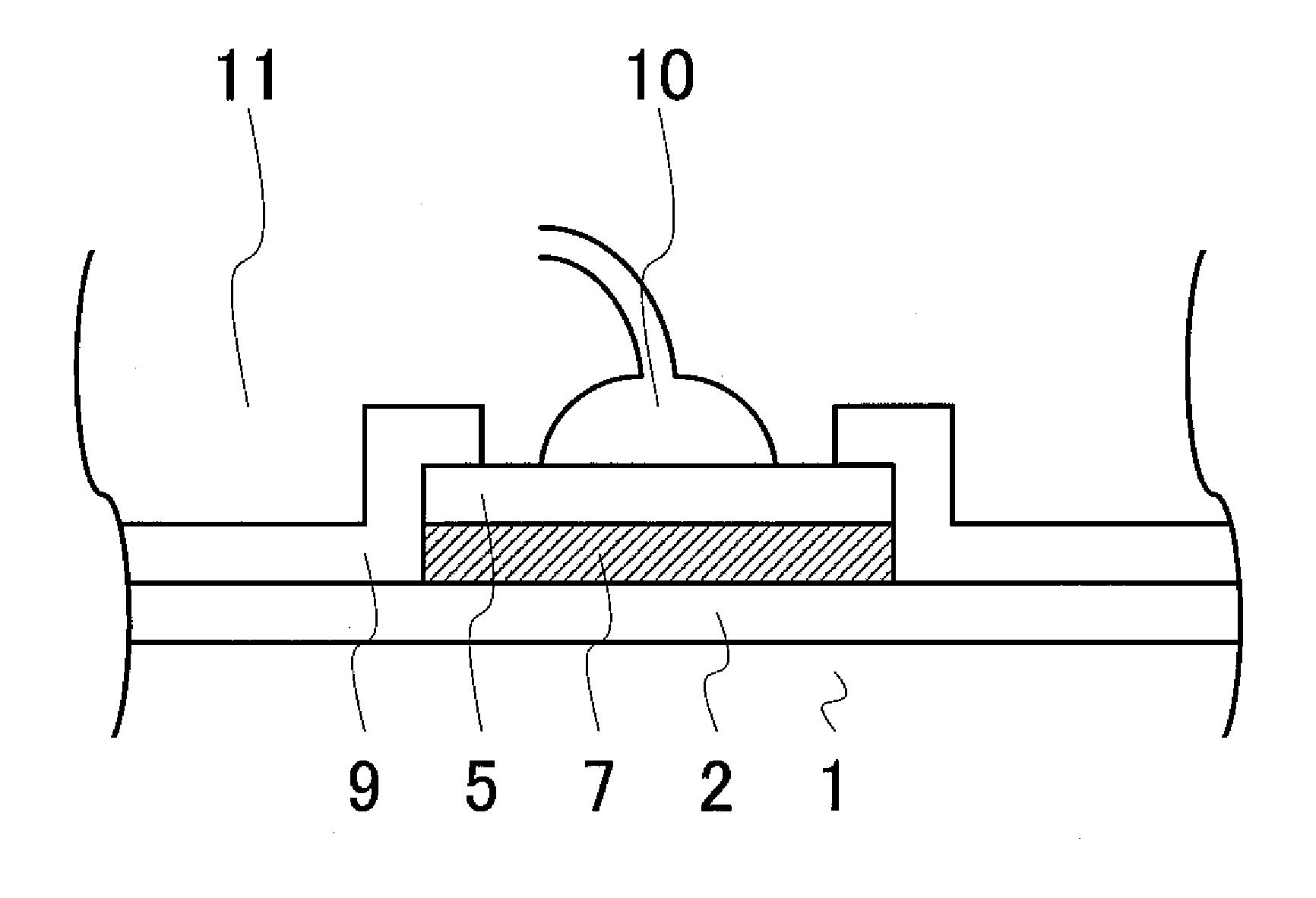
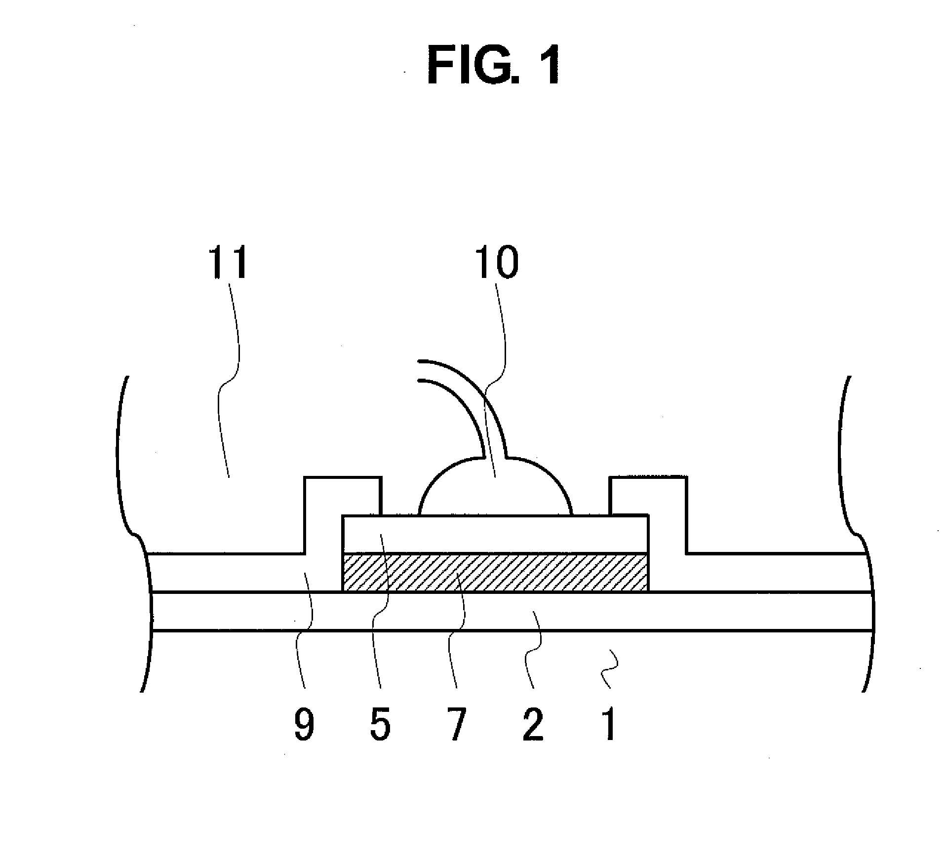
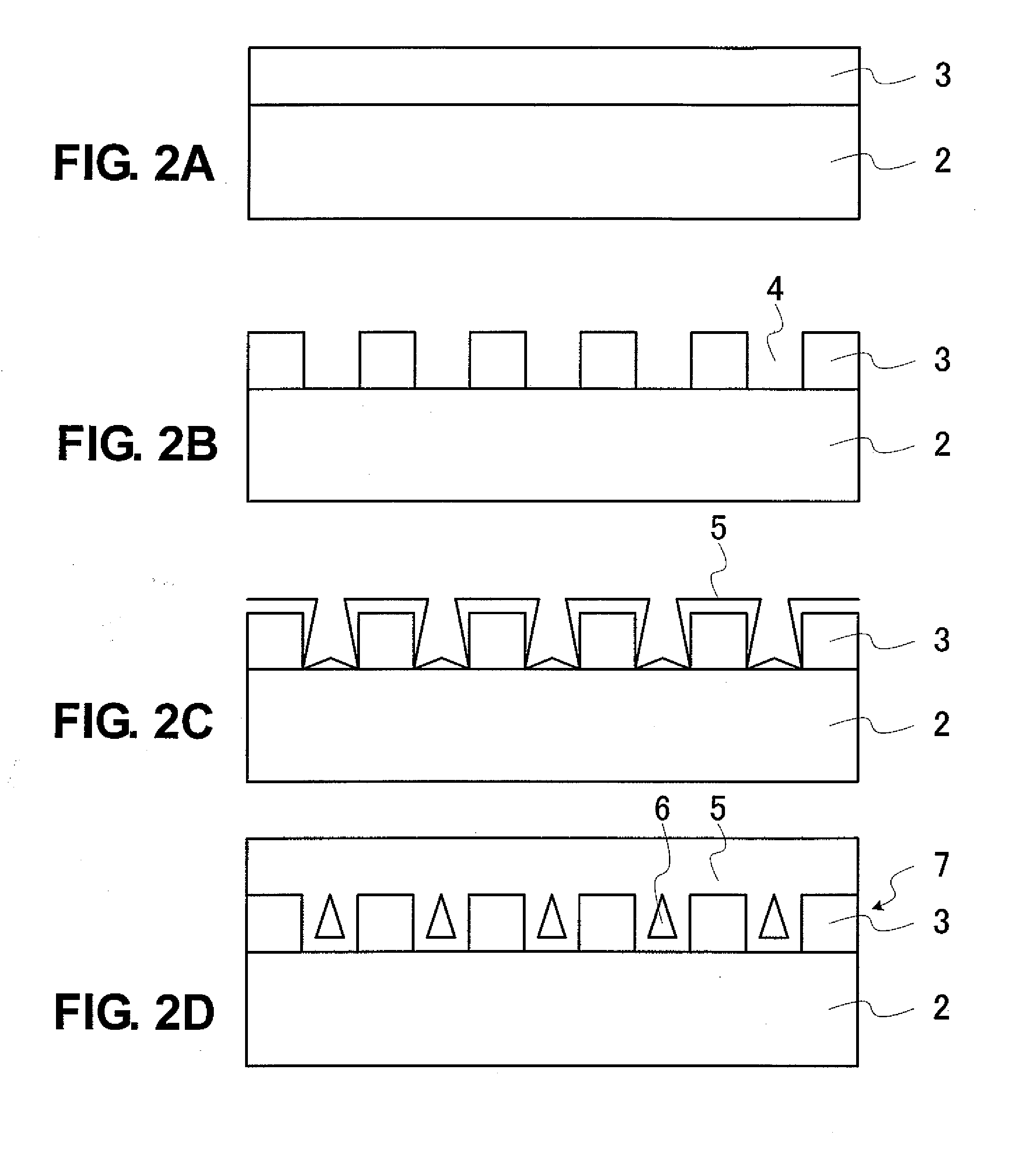
[0043][Modification 9]FIGS. 10 to 14 are partial sectional views illustrating a film structure of the region of the porous metal film 7 of the semiconductor device according to the present invention, and a method of manufacturing the semiconductor device according to the present invention. FIG. 10 illustrates the insulating film 2 onto which conductive paste 16 is applied. The conductive paste is a liquid mixture containing a plurality of first metal nanoparticles 12 and an organic binder 15, and the metal nanoparticles 12 are dispersed in the liquid mixture. Since baking of the conductive paste causes decomposition of the organic binder, degassing in a vacuum atmosphere, as illustrated in FIGS. 11 and 12, enables bonding between the plurality of metal nanoparticles 12, forming inter-particle voids 14 among the particles. The porous metal film 7 including the metal nanoparticles and the inter-particle voids is thus formed. Here, the porous metal film 7 can be porous by being formed ...


PUM

PropertyMeasurementUnit
gas pressureaaaaaaaaaa
pressureaaaaaaaaaa
insulatingaaaaaaaaaa

Abstract

The semiconductor device includes: a semiconductor substrate; an insulating film provided on a surface of the semiconductor substrate; a porous metal film provided on the insulating film; a protective film provided on the porous metal film, and having an opening portion for defining a pad region; and a wire wire-bonded to the porous metal film in the pad region. The stress generated by the impact of wire-bonding is mostly absorbed in the porous metal film owing to the distortion of the porous metal film, preventing generation of cracks in the insulating film.

Description

BACKGROUND OF THE INVENTION[0001]1. Field of the Invention[0002]The present invention relates to a semiconductor device having a pad used in wire-bonding and a method of manufacturing the semiconductor device.[0003]2. Description of the Related Art[0004]A conventional semiconductor device having a pad is described. FIG. 9 illustrates a sectional view of a pad portion of the conventional semiconductor device. In this example, an opening portion of a protective film 93 on an uppermost metal film 92, which is provided on an upper surface of an insulating film 91, is defined as the pad. A wire 94 is connected to the pad by wire-bonding (for example, see Japanese Published Patent Application No. 03-049231).[0005]However there has been a risk that in a conventional semiconductor device having a pad, due to the stress generated by the impact of wire-bonding, cracks might be found in the pad made of the metal film 92 or in the insulating film 91 under the pad, which has also been a problem....

Claims


Application Information

Patent Timeline
Patent Type & Authority Applications(United States)
IPC IPC(8): H01L23/49H01L21/60
CPCH01L24/05H01L24/43H01L2224/48463H01L2924/00014H01L24/48H01L2224/02166H01L2224/05H01L2924/01033H01L24/03H01L2224/04042H01L2224/05198H01L2224/45099H01L2924/181H01L2224/43H01L2924/00H01L2224/05395H01L2224/052
Inventor AKINO, MASARU
Owner ABLIC INC
Why Eureka
Try Eureka