Pixel array of fringe field switching liquid crystal display panel and driving method thereof

a fringe field switching and liquid crystal display panel technology, applied in the direction of electric digital data processing, instruments, computing, etc., can solve the problems of high power consumption of driving the array substrate, complicated driving methods of the array substrate, and driving up the cost of integrated circuits (ics), so as to improve the power consumption of the fringe field switching liquid crystal display panel, simplify the driving method, and reduce the cost of driving ics

Active Publication Date: 2012-10-04
AU OPTRONICS CORP
View PDF3 Cites 15 Cited by
  • Summary
  • Abstract
  • Description
  • Claims
  • Application Information

AI Technical Summary

Benefits of technology

[0009]In the pixel array of the fringe field switching liquid crystal display panel, the common lines, which may be driven independently, are employed with the allocation approaches of the common electrodes in the sub-pixel regions for presenting a dot inversion driving effect by a simplified driving method. Costs of the driving ICs may then be reduced, and the power consumption of the fringe field switching liquid crystal display panel may be also improved.

Problems solved by technology

However, in conventional fringe field switching liquid crystal display panels, a plurality of common lines, which connect to the common electrodes, are electrically connected to each other and may not be driven independently.
Therefore, driving methods of the array substrate have to be more complicated for presenting different display driving effects, such as a dot inversion driving effect.
This results in driving up the cost of integrated circuits (ICs) and high power consumption for driving the array substrate, also leads away from goals of energy saving and carbon reduction.

Method used


Image

  • Pixel array of fringe field switching liquid crystal display panel and driving method thereof
  • Pixel array of fringe field switching liquid crystal display panel and driving method thereof
  • Pixel array of fringe field switching liquid crystal display panel and driving method thereof

Examples


first embodiment

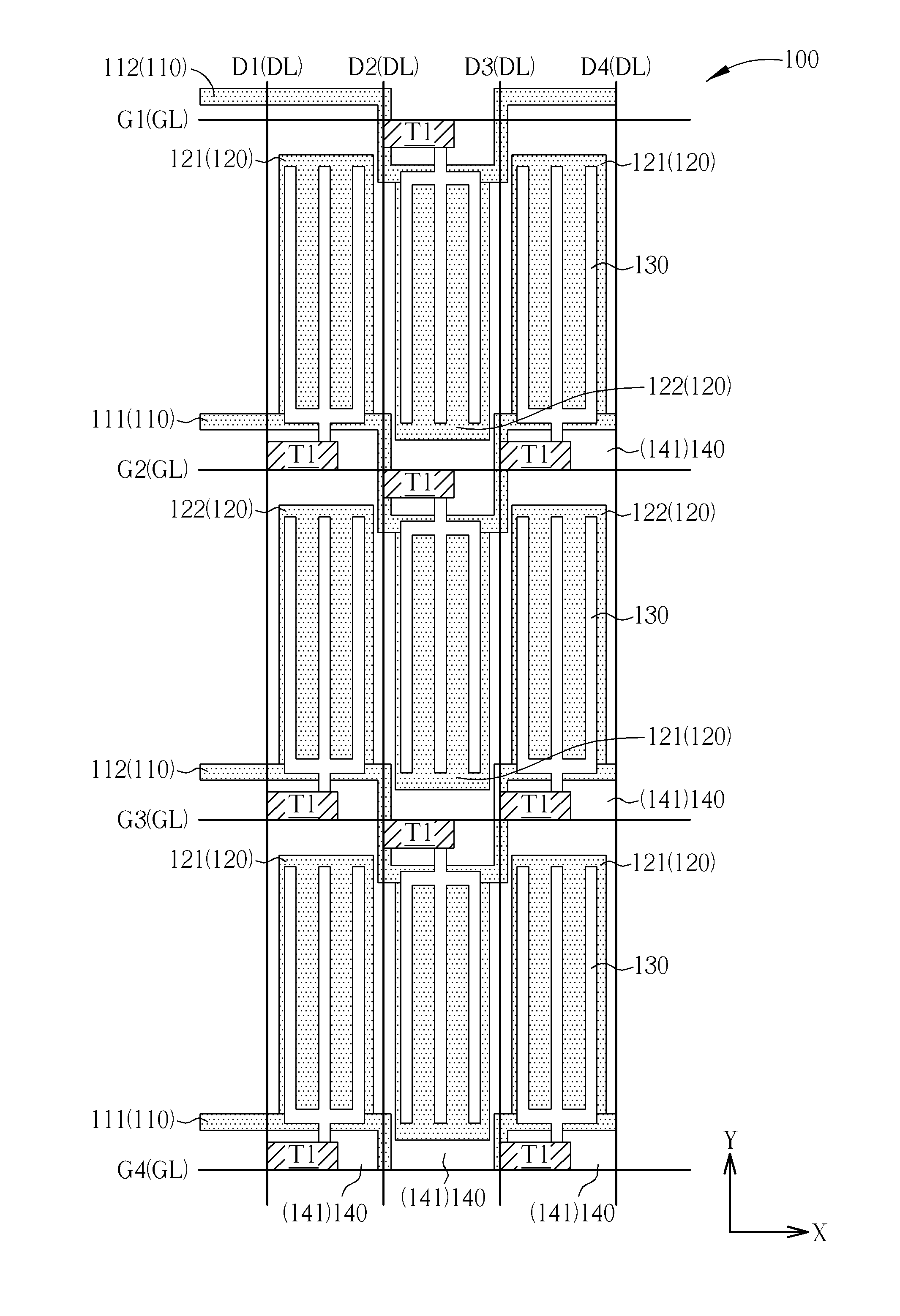
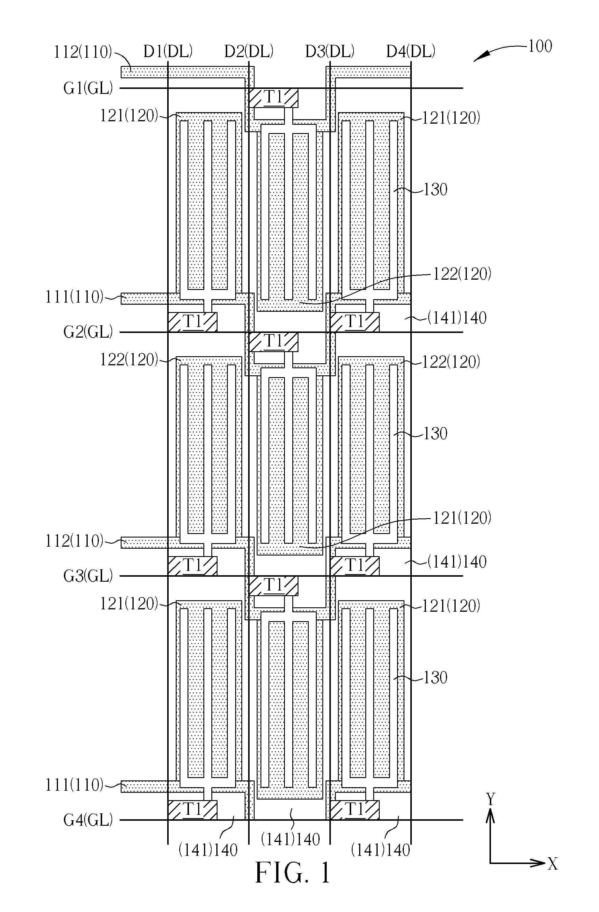
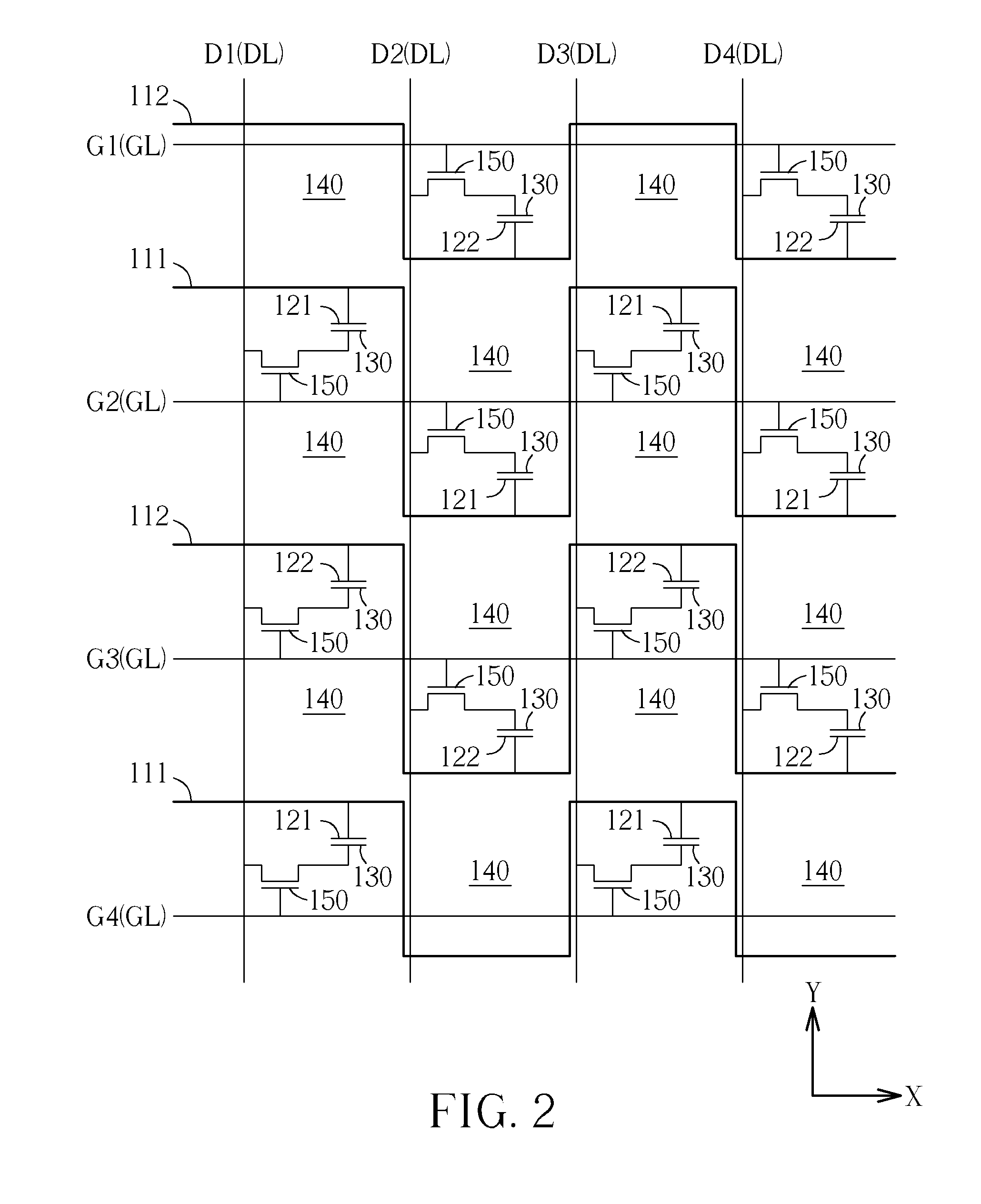
[0026]Please refer to FIGS. 1-3. FIG. 1 is a schematic diagram illustrating a pixel array of a fringe field switching liquid crystal display panel according to a FIG. 2 is a schematic diagram illustrating electrical circuits of the pixel array of the fringe field switching liquid crystal display panel according to this embodiment. FIG. 3 is a schematic diagram illustrating common lines and common electrodes of the fringe field switching liquid crystal display panel according to this embodiment. Please note that the figures are only for illustration and the figures may not be to scale. The scale may be further modified according to different design considerations. As shown in FIG. 1, in this embodiment, a pixel array 100 of a fringe field switching liquid crystal display panel is provided. The pixel array 100 includes a plurality of gate lines GL, a plurality of data lines DL, a plurality of pixel electrodes 130, and a plurality of common lines 110. The gate lines GL are disposed pa...

second embodiment

[0030]Please refer to FIG. 7, and refer to FIGS. 5-6 together. FIG. 7 is a schematic diagram illustrating timings of a driving method of a fringe field switching liquid crystal display panel according to the In the driving method of the fringe field switching liquid crystal display panel of this embodiment, the structure and properties of the pixel array 200 have been detailed above and will not be redundantly described. As shown in FIG. 7 and FIG. 5, in this embodiment, the driving method of the fringe field switching liquid crystal display panel includes providing a plurality of common signals Vcom[m] to the common lines 110 for driving the pixel array 200, wherein within one frame time F[N], a level of the common signals Vcom[m] provided to the odd common lines 110 is different from a level of the common signals Vcom[m] provided to the even common lines 110. Additionally, a condition of high / low level of the common signals Vcom[m] provided to the common lines 110 in one frame ti...

third embodiment

[0040]The first common electrode 721 may include one sub common electrode 721A, one sub common electrode 721B, and one sub common electrode 721C respectively disposed correspondingly in the sub-pixel region 741, the sub-pixel region 742, and the sub-pixel region 743. The second common electrode 722 may include one sub common electrode 722A, one sub common electrode 722B, and one sub common electrode 722C respectively disposed correspondingly in the sub-pixel region 741, the sub-pixel region 742, and the sub-pixel region 743. Additionally, each of the pixel electrodes 730 in this embodiment is respectively disposed in each of the sub-pixel regions 741, each of the sub-pixel regions 742, and each of the sub-pixel regions 743. The pixel array 700 may further include a plurality of switching devices T7 respectively disposed correspondingly to each of the sub-pixel regions 741, each of the sub-pixel regions 742, and each of the sub-pixel regions 743. Each of the switching devices T7 is e...


PUM

PropertyMeasurementUnit
transparent conductiveaaaaaaaaaa
frame timeaaaaaaaaaa
conductiveaaaaaaaaaa

Abstract

A pixel array of a fringe field switching (FFS) liquid crystal display panel includes a plurality of gate lines, a plurality of data line, a plurality of pixel electrodes, a plurality of common lines, and a plurality of pixel units aligned in an array configuration. The gate lines are disposed parallel to each other along a first direction. The data lines are disposed parallel to each other along a second direction. Each of the pixel units includes at least one sub-pixel region. The common lines are disposed along the first direction and electrically isolated from each other. Each of the common lines includes a plurality of common electrodes extending along the second direction. The two adjacent common electrodes of each common line are respectively disposed in the two adjacent pixel units which are located in different rows.

Description

CROSS REFERENCE TO RELATED APPLICATIONS[0001]This application is a continuation in part of U.S. application Ser. No. 13 / 172,766, filed 2011 Jun. 29.BACKGROUND[0002]1. Technical Field[0003]The disclosure relates to a pixel array of a fringe field switching liquid crystal display panel and a driving method thereof, and more particularly, to a pixel array of a fringe field switching liquid crystal display panel with a plurality of common lines and a driving method thereof.[0004]2. Description of the Related Art[0005]Liquid crystal display panels are applied in many kinds of consumer electronics such as flat TVs, laptop computers, and cell phones. Fringe field switching (FFS) liquid crystal display panels have been developed for improving narrow viewing angle issues in liquid crystal display panels. The main features of the FFS liquid crystal display panel include that common electrodes and pixel electrodes are disposed in different layers of an array substrate (also called a thin film ...

Claims


Application Information

Patent Timeline
Patent Type & Authority Applications(United States)
IPC IPC(8): G09G5/00G09G3/36G02F1/1343
CPCG09G3/3614G09G3/3655G09G2300/0426G09G2310/08G02F2001/134372G02F1/1343G09G3/36G09G5/00G02F1/136286G09G2330/021G02F1/134372
Inventor PAI, CHENG-CHIU
Owner AU OPTRONICS CORP
Why Eureka
Try Eureka