Organic light emitting diode display

a light-emitting diode and organic technology, applied in the direction of organic semiconductor devices, diffusing elements, planar/plate-like light guides, etc., can solve the problems of deteriorating light efficiency and deteriorating organic light-emitting elements, and achieve the effect of improving light-emitting efficiency

Active Publication Date: 2012-10-11
SAMSUNG DISPLAY CO LTD
View PDF3 Cites 54 Cited by
  • Summary
  • Abstract
  • Description
  • Claims
  • Application Information

AI Technical Summary

Benefits of technology

[0021]According to the exemplary embodiments, light efficiency may be improved by dispersing scattering materials in at lea...

Problems solved by technology

The organic light emitting element may deteriorate due to internal and external factors.
Thus, the light emitted from the...

Method used


Image

  • Organic light emitting diode display
  • Organic light emitting diode display
  • Organic light emitting diode display

Examples


Embodiment Construction

[0028]The present invention will be described more fully hereinafter with reference to the accompanying drawings, in which exemplary embodiments of the invention are shown. As those skilled in the art would realize, the described embodiments may be modified in various different ways, all without departing from the spirit or scope of the present invention.

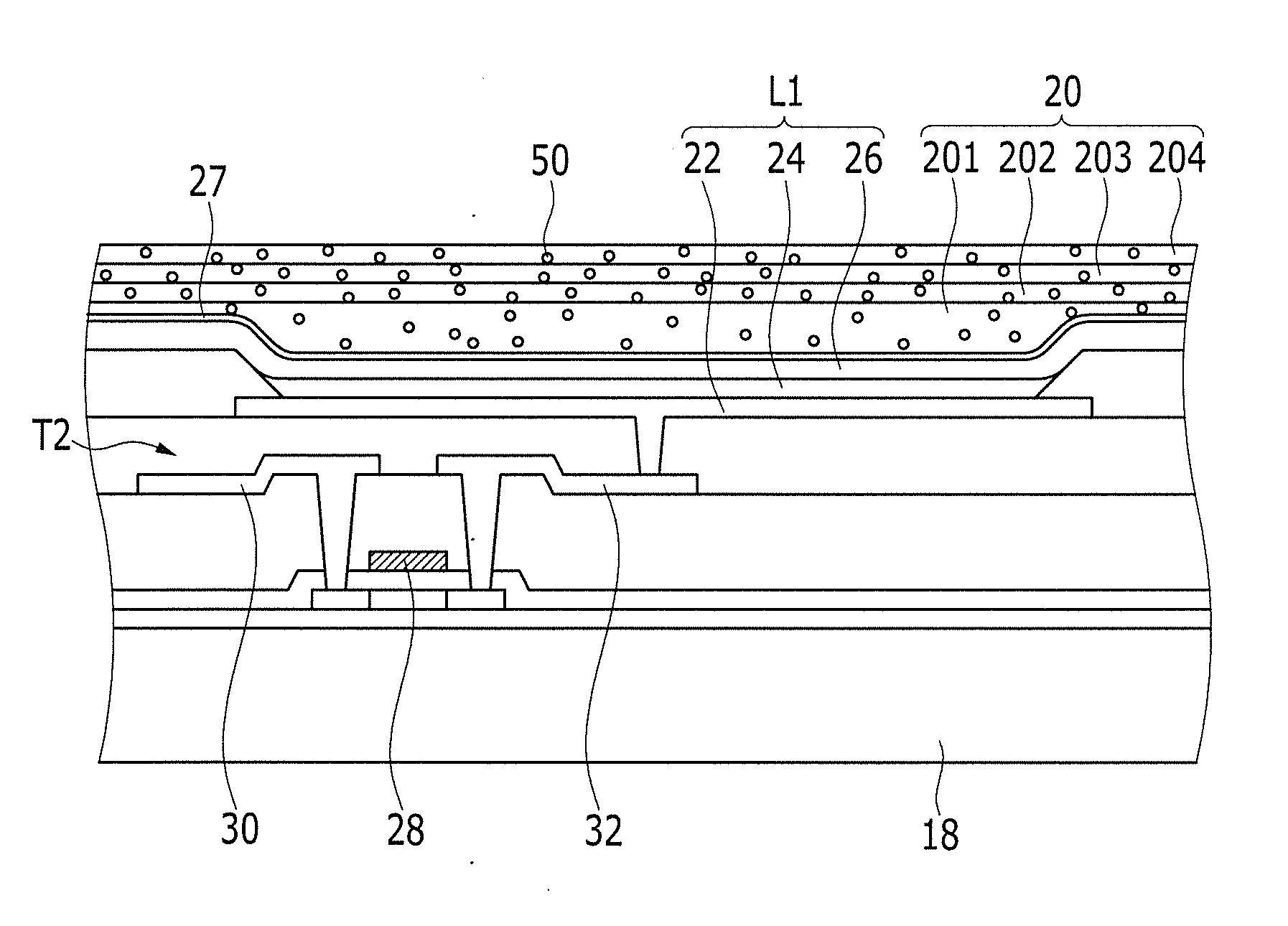
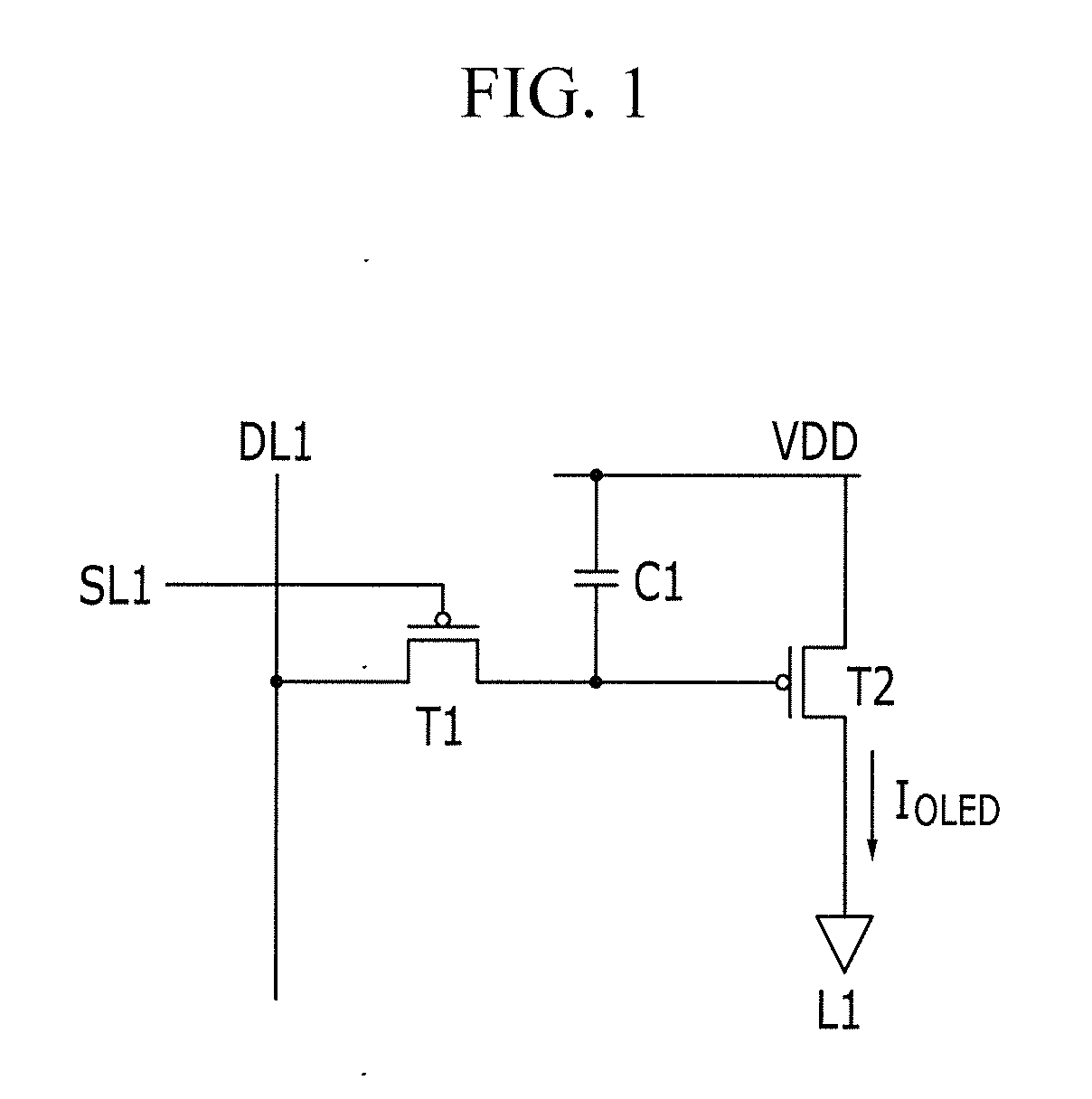
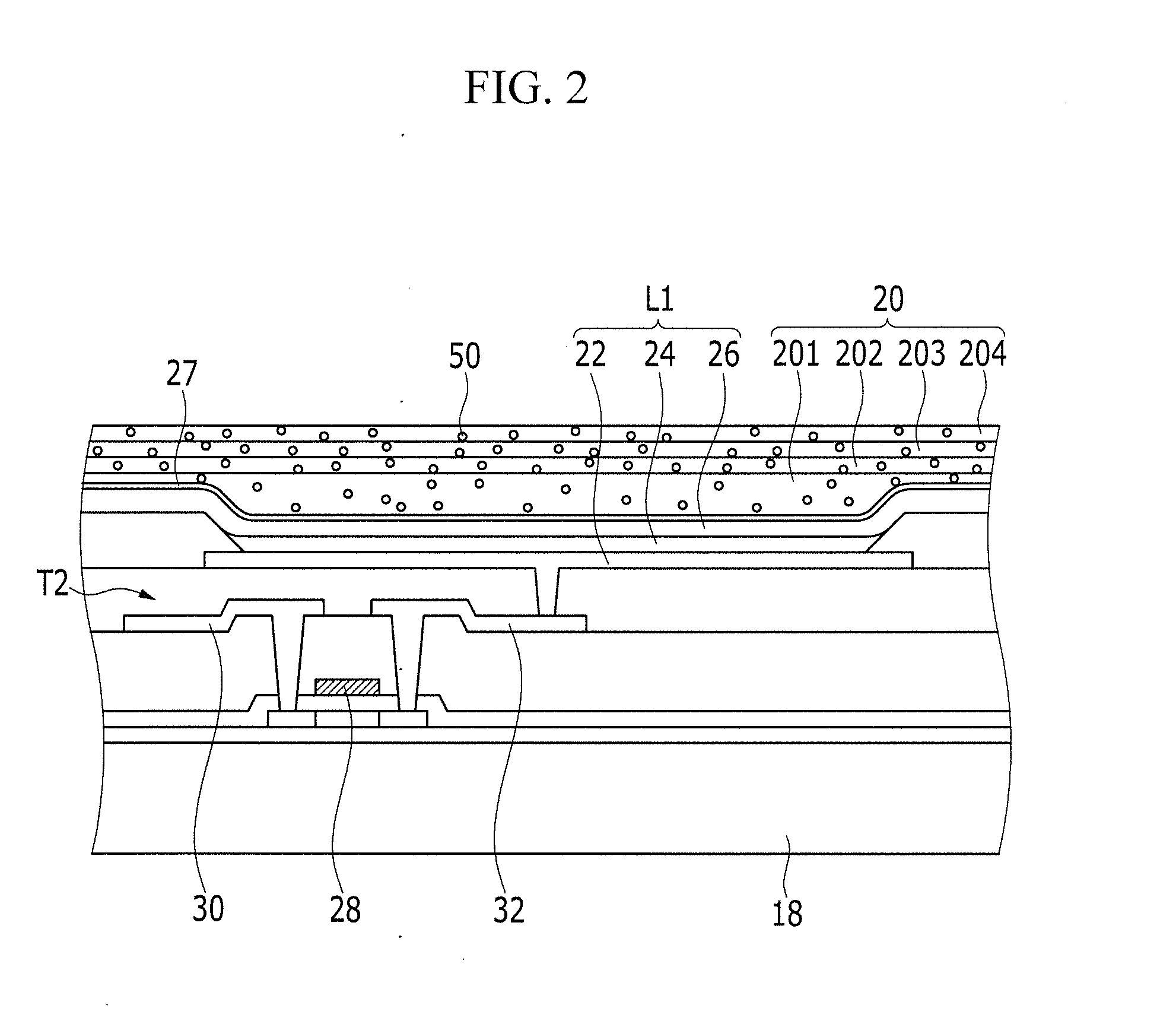
[0029]FIG. 1 is a schematic circuit diagram of a pixel circuit of an organic light emitting diode (OLED) display according to an exemplary embodiment, and FIG. 2 is a cross-sectional view of the OLED display of FIG. 1.

[0030]As shown in FIG. 1 and FIG. 2, each pixel of the OLED display is formed of an organic light emitting element L1 and a driving circuit. The organic light emitting element L1 includes a first pixel electrode (e.g., hole injection electrode) 22, an organic emission layer 24, and a second pixel electrode (e.g., electron injection electrode) 26.

[0031]In addition to an emission layer (not shown) that emits light, the o...


PUM


Abstract

An organic light-emitting diode (OLED) display according to an exemplary embodiment may include: a substrate and an organic light emitting element on the substrate; a thin film encapsulation layer on the substrate and covering the organic light emitting element; and one or more scattering materials dispersed in the thin film encapsulation layer. According to the exemplary embodiment, light efficiency may be improved by dispersing scattering materials in at least one of an organic layer or an inorganic layer forming a thin film encapsulation layer with a large refractive index difference.

Description

CROSS-REFERENCE TO RELATED APPLICATION[0001]This application claims priority to and the benefit of Korean Patent Application No. 10-2011-0033396 filed in the Korean Intellectual Property Office on Apr. 11, 2011, the entire content of which is incorporated herein by reference.BACKGROUND[0002]1. Field[0003]Aspects of embodiments according to the present invention relate generally to an organic light emitting diode (OLED) display.[0004]2. Description of the Related Art[0005]An organic light emitting diode (OLED) display includes organic light emitting elements formed of a hole injection electrode, an organic emission layer, and an electron injection electrode. With the OLED display, electrons and holes are combined with each other in the organic emission layer to thereby generate excitons. When the excitons transition from the excited state to the ground state, energy is released so as to emit light, and images are displayed by the emitted light.[0006]An OLED display is a flat panel di...

Claims


Application Information

Patent Timeline
IPC IPC(8): H01L33/58
CPCH01L27/3244H01L51/5256H01L2251/5369H01L51/5275H01L51/5268H10K59/12H10K50/8445H10K50/854H10K50/858H10K2102/331G02B5/02G02B6/004
Inventor KWACK, JIN-HOHAN, DONG-WON
Owner SAMSUNG DISPLAY CO LTD
Why Eureka
Try Eureka