Display panel and testing method thereof

a display panel and test method technology, applied in electrical testing, measurement devices, instruments, etc., can solve problems such as line defects in scan lines in display panels

Active Publication Date: 2012-10-18
AU OPTRONICS CORP
View PDF2 Cites 107 Cited by
  • Summary
  • Abstract
  • Description
  • Claims
  • Application Information

AI Technical Summary

Benefits of technology

[0011]Based on the above, the testing line and the testing pad are disposed in the non-display region, and the testing line crosses over the scan lines, as described in the embodiments of the invention. When one of the scan lines in the display panel is found to have a line defect, the melting and connecting process can be directly performed on an area where the testing line crosses over the scan line having the line defect, such that the testing line is electrically connected to the scan line having the line defect. After the testing signal is input to the scan line having the line defect, the testing signal can be transmitted to the testing pad through the defective scan line and the testing line. Thus, the output signal received from the testing pad can be directly measured. That is to say, it is not necessary to cleave and pierce the substrate in the display panel described in the embodiments of the invention, and the output signal of the scan line can still be measured.

Problems solved by technology

Here, one of the scan lines in the display panel has a line defect.

Method used


Image

  • Display panel and testing method thereof
  • Display panel and testing method thereof
  • Display panel and testing method thereof

Examples


Embodiment Construction

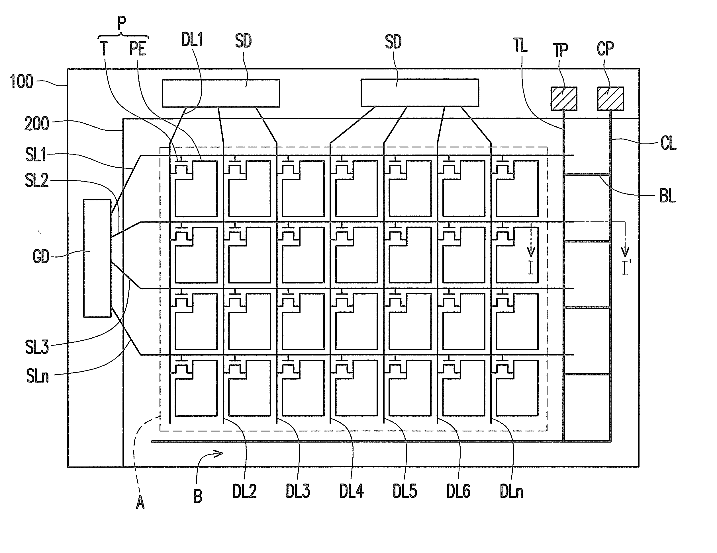
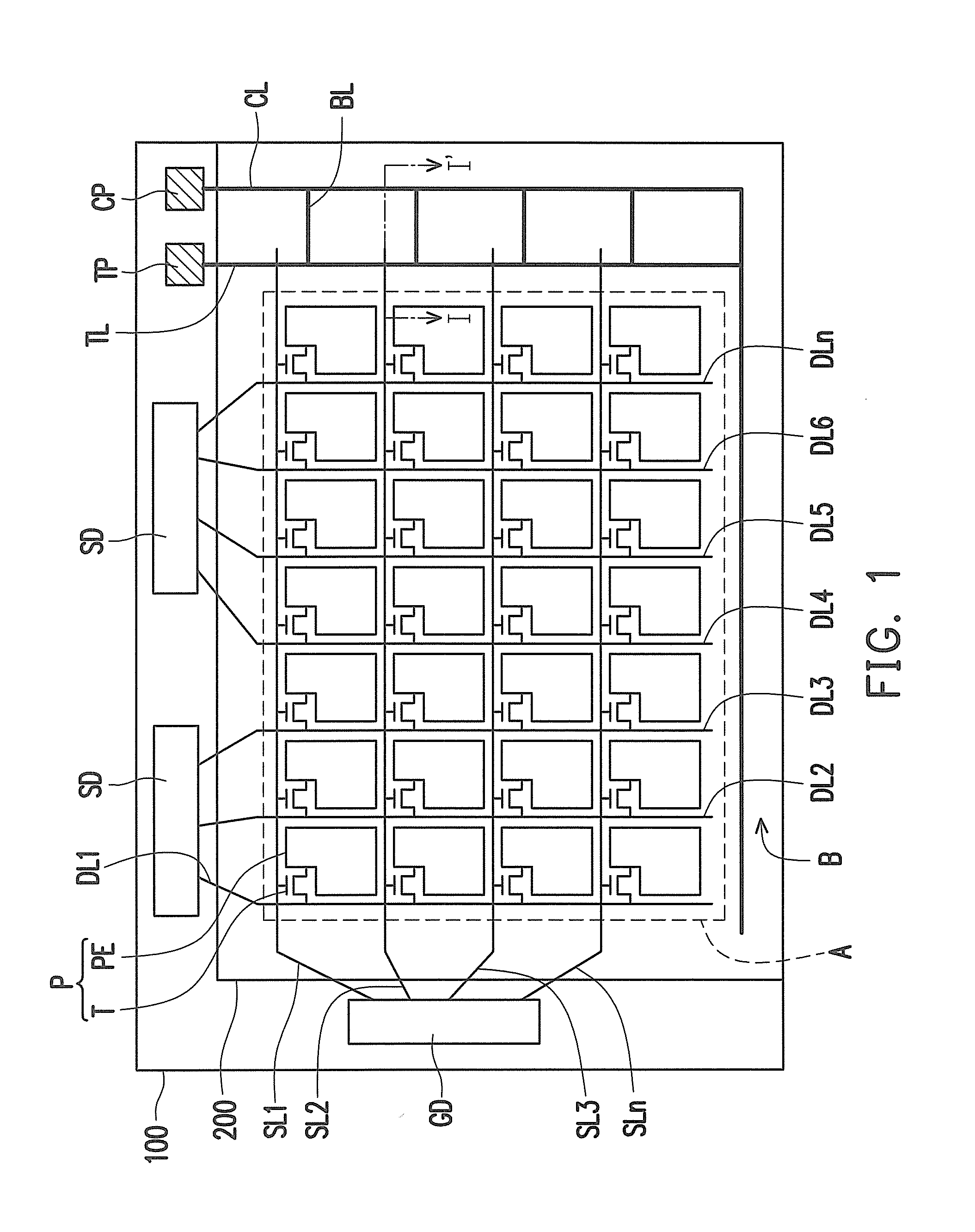
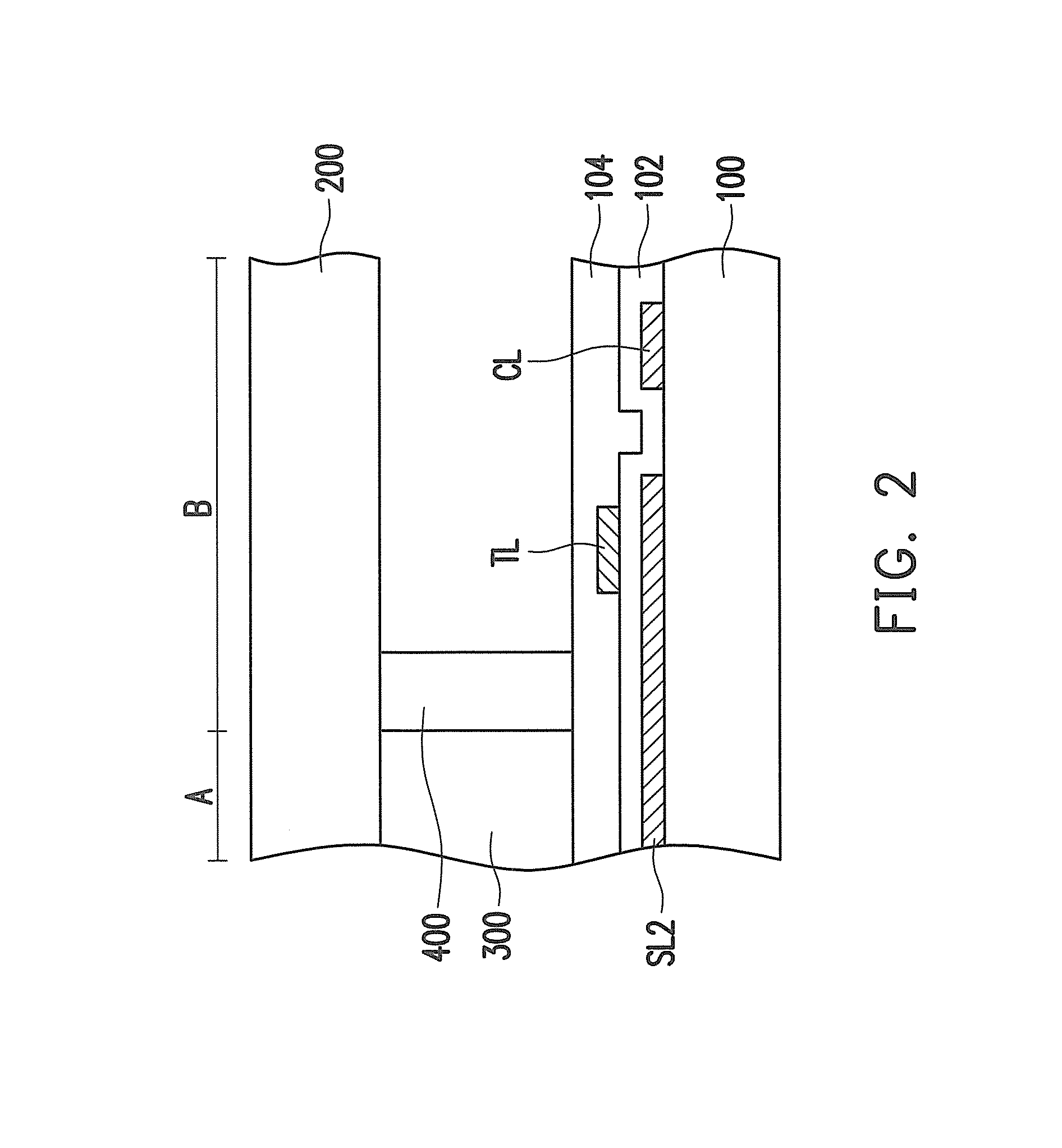
[0022]FIG. 1 is a schematic top view illustrating a display panel according to an embodiment of the invention. FIG. 2 is a schematic cross-sectional view taken along a sectional line I-I′ depicted in FIG. 1. With reference to FIG. 1 and FIG. 2, the display panel of this embodiment has a display region A and a non-display region B. Besides, the display panel includes a first substrate 100, a second substrate 200, and a display medium 300 located between the first and second substrates 100 and 200. The display panel further includes a plurality of scan lines SL1˜SLn, a plurality of data lines DL1˜DLn, a plurality of pixel units P, at least one testing line TL, and at least one testing pad TP.

[0023]The first substrate 100 and the second substrate 200 are opposite to each other. In addition, the first and second substrates 100 and 200 can be transparent substrates. Alternatively, one of the first and second substrates 100 and 200 is a transparent substrate, while the other is a non-tran...


PUM


Abstract

A display panel and a testing method of the display panel are provided. The display panel has a display region and a non-display region and includes a first substrate, a second substrate, and a display medium. The display panel further includes scan lines, data lines, pixel units, at least one testing line, and at least one testing pad. The scan lines and the data lines are located on the first substrate within the display region. The pixel units are located on the first substrate within the display region. Each pixel unit electrically connects one of the scan lines and one of the data lines. The testing line is located on the first substrate within the non-display region, crosses over the scan lines, and is insulated from the scan lines. The testing pad is located on the first substrate within the non-display region and electrically connected to the testing line.

Description

CROSS-REFERENCE TO RELATED APPLICATION[0001]This application claims the priority benefit of Taiwan application serial no. 100112993, filed on Apr. 14, 2011. The entirety of the above-mentioned patent application is hereby incorporated by reference herein and made a part of this specification.BACKGROUND OF THE INVENTION[0002]1. Field of the Invention[0003]The invention relates to a display panel and a testing method thereof.[0004]2. Description of Related Art[0005]In general, a conventional liquid crystal display (LCD) panel is constituted by a color filter (C / F), a thin film transistor (TFT) array substrate, and a liquid crystal layer sandwiched therebetween. Particularly, the TFT array substrate has an active region and a peripheral circuit region. A plurality of pixel arrays are disposed in the active region. Lead lines, bonding pads, and testing transistors are disposed in the peripheral circuit region.[0006]When the TFT array substrate is being formed, electrical inspection is o...

Claims


Application Information

Patent Timeline
Patent Type & Authority Applications(United States)
IPC IPC(8): G01R31/02
CPCG09G3/006G09G2310/02G09G2300/0426
Inventor SHEN, CHUNG-MING
Owner AU OPTRONICS CORP
Why Eureka
Try Eureka