Semiconductor memory device and method of reading out the same

a memory device and memory technology, applied in the field of memory devices and memory devices, can solve problems such as data being erroneously read out, and achieve the effect of reducing the read tim

Active Publication Date: 2012-10-25
SK HYNIX INC
View PDF2 Cites 14 Cited by
  • Summary
  • Abstract
  • Description
  • Claims
  • Application Information

AI Technical Summary

Benefits of technology

[0007]Exemplary embodiments relate to a semiconductor memory device and a method of reading out the same, which are capable of reducing the read time by using a cache read method of reading out normal data from a memory cell using a normal read voltage and of reading out over-sampling data, indicating whether the threshold voltage of the memory cell falls within a specific voltage range, using a first read voltage lower than the normal read voltage and a second read voltage higher than the normal read voltage in a read operation.

Problems solved by technology

In a read operation, data may be erroneously read out from memory cells having threshold voltages included in the overlapped parts.

Method used


Image

  • Semiconductor memory device and method of reading out the same
  • Semiconductor memory device and method of reading out the same
  • Semiconductor memory device and method of reading out the same

Examples


Embodiment Construction

[0018]Hereinafter, some exemplary embodiments of the present disclosure will be described in detail with reference to the accompanying drawings. The figures are provided to allow those having ordinary skill in the art to understand the scope of the embodiments of the disclosure.

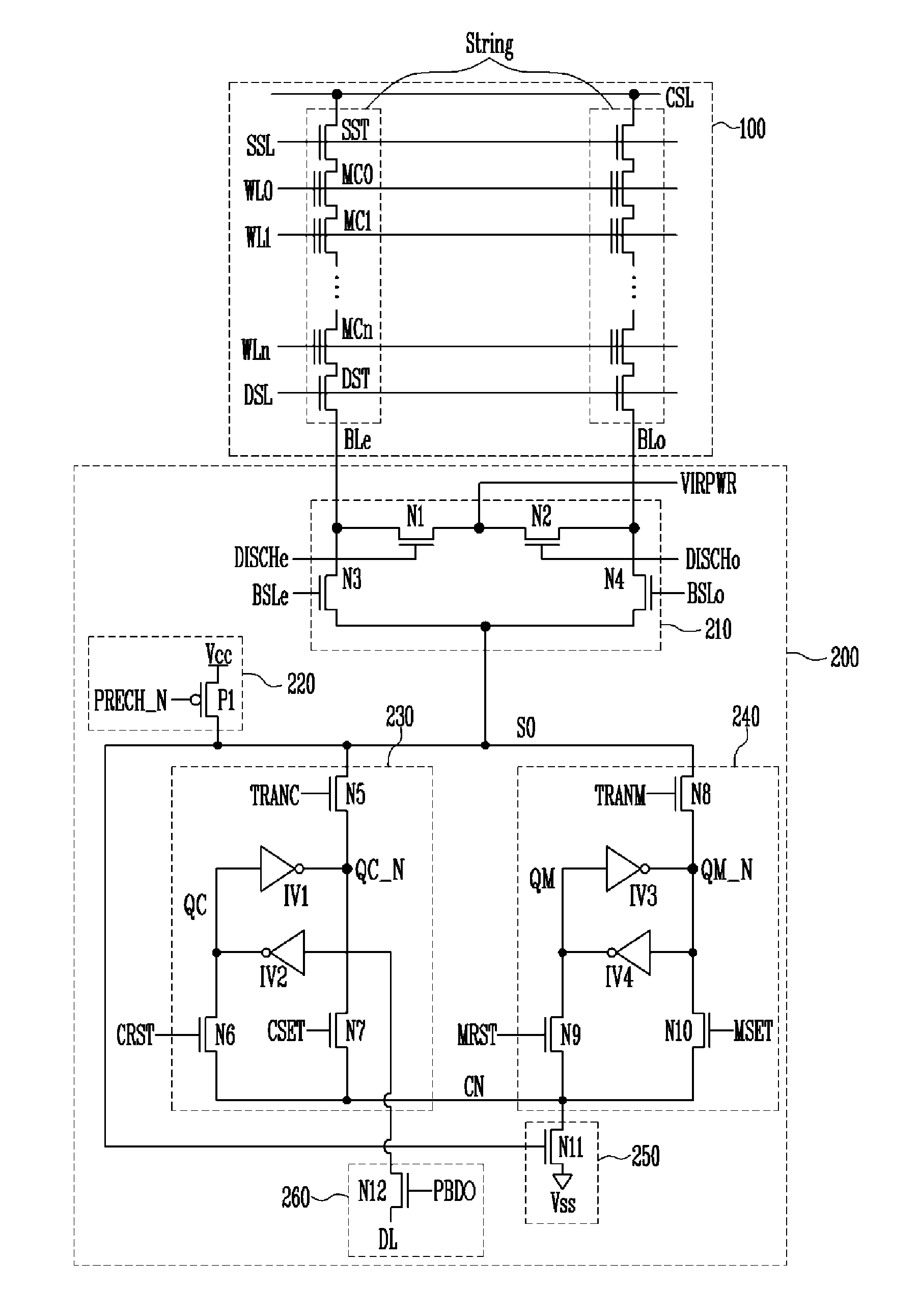
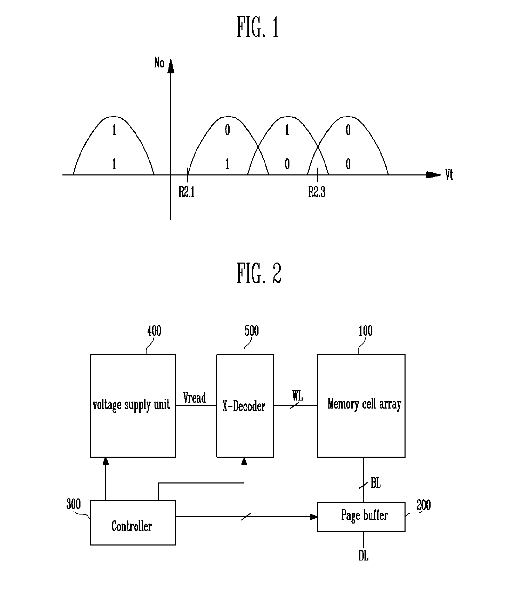
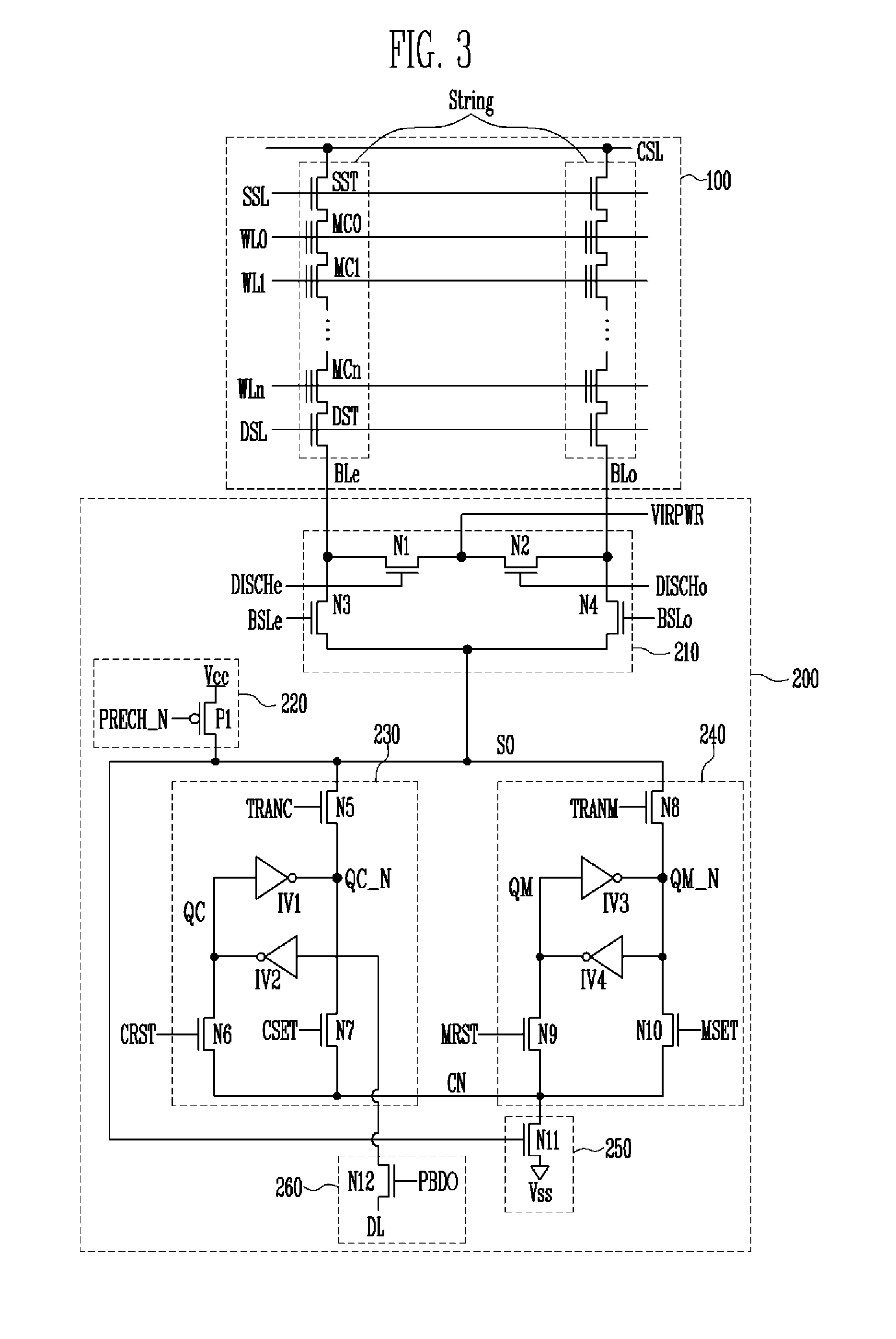
[0019]FIG. 2 shows the configuration of a semiconductor memory device according to an exemplary embodiment of the present invention.

[0020]Referring to FIG. 2, the semiconductor memory device includes a memory cell array 100, a page buffer 200, a controller 300, a voltage supply unit 400, and an X decoder 500.

[0021]The memory cell array 100 includes a plurality of memory cell for storing data.

[0022]The page buffer 200 is coupled between a data line DL and the bit line BL of the memory cell array 100 and is configured to read out normal read data and over-sampling read data by sensing a voltage level of the bit line BL of the memory cell array 100 in response to a plurality of page buffer control signals from t...


PUM


Abstract

A semiconductor memory device includes a memory cell array configured to include memory cells, peripheral circuits configured to read out data stored in a selected memory cell in a read operation, and a controller configured to control the peripheral circuits so that the peripheral circuits sense a voltage level of the bit line when a first read voltage of the read voltages is supplied to the word line and the peripheral circuits sense voltage levels of the bit line when a second read voltage lower than the first read voltage by a specific level and a third read voltage higher than the first read voltage by the specific level are supplied to the word line in order to determine whether a threshold voltage of the selected memory cell falls within a set voltage distribution in the read operation.

Description

CROSS-REFERENCE TO RELATED APPLICATION[0001]Priority is claimed to Korean patent application number 10-2011-0038305 filed on Apr. 25, 2011, the entire disclosure of which is incorporated herein by reference in its entirety.BACKGROUND[0002]Exemplary embodiments relate generally to a semiconductor memory device and a method of reading out the same, and more particularly to a semiconductor memory device of reading out normal read data and over-sampling read data in a read operation and a method of reading out the same.[0003]Semiconductor memory devices can be divided into a volatile memory device and a non-volatile memory device. The volatile memory device requires power to retain the stored information. On the other hands, the non-volatile memory device can retain the stored information even in absence of power supply.[0004]With increasing demand for highly integrated memory devices, semiconductor memory devices in which multi-bit data are stored in a single memory cell are generally ...

Claims


Application Information

Patent Timeline
Patent Type & Authority Applications(United States)
IPC IPC(8): G11C7/10G11C7/00
CPCG11C7/00G11C16/0483G11C11/5642G11C7/10G11C16/06G11C16/26
Inventor YANG, IN GONKIM, DUCK JUCHA, JAE WONAHN, SUNG HOONJEON, TAE HO
Owner SK HYNIX INC
Why Eureka
Try Eureka