

Semiconductor memory device and repair method thereof
a memory device and semiconductor technology, applied in the direction of semiconductor devices, semiconductor/solid-state device details, instruments, etc., can solve the problems of reducing the yield of semiconductor memory devices, memory cell defects may occur, and the proportion of the line width of circuitry is decreased, so as to achieve the effect of simple repairing process
- Summary
- Abstract
- Description
- Claims
- Application Information
AI Technical Summary
Benefits of technology
Problems solved by technology
Method used
Image

Examples
Embodiment Construction
[0030]Exemplary embodiments of the present invention will be described below in more detail with reference to the accompanying drawings. The present invention may, however, be embodied in different forms and should not be construed as limited to the embodiments set forth herein. Rather, these embodiments are provided so that this disclosure will be thorough and complete, and will fully convey the scope of the present invention to those skilled in the art. Throughout the disclosure, like reference numerals refer to like parts throughout the various figures and embodiments of the present invention.
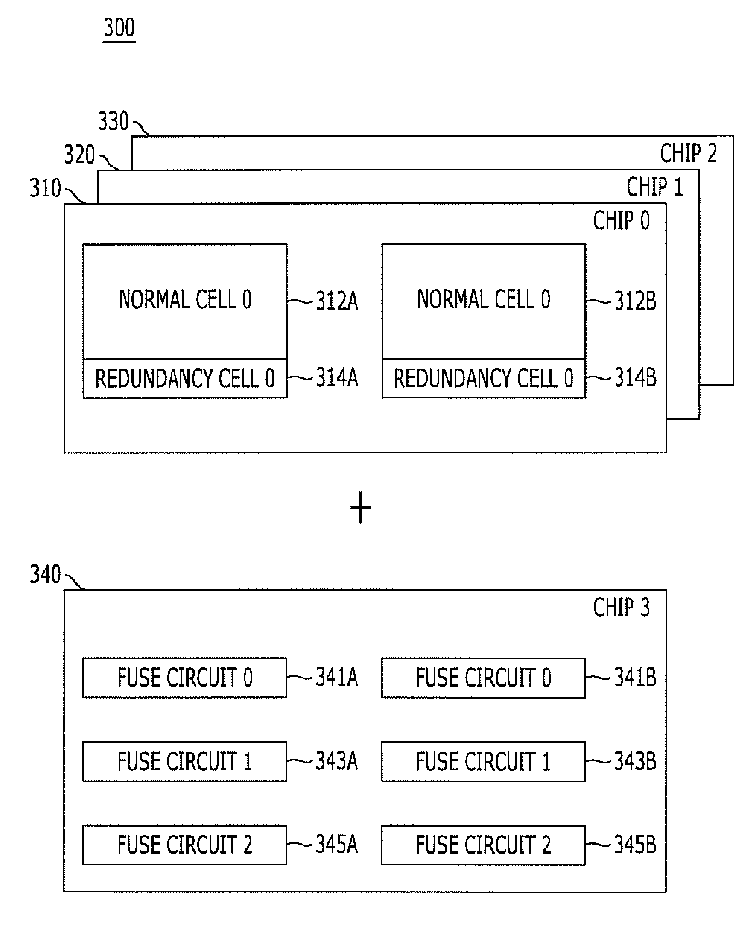
[0031]For illustration purposes, a semiconductor memory device including four semiconductor chips stacked together in accordance with an embodiment of the present invention is described.
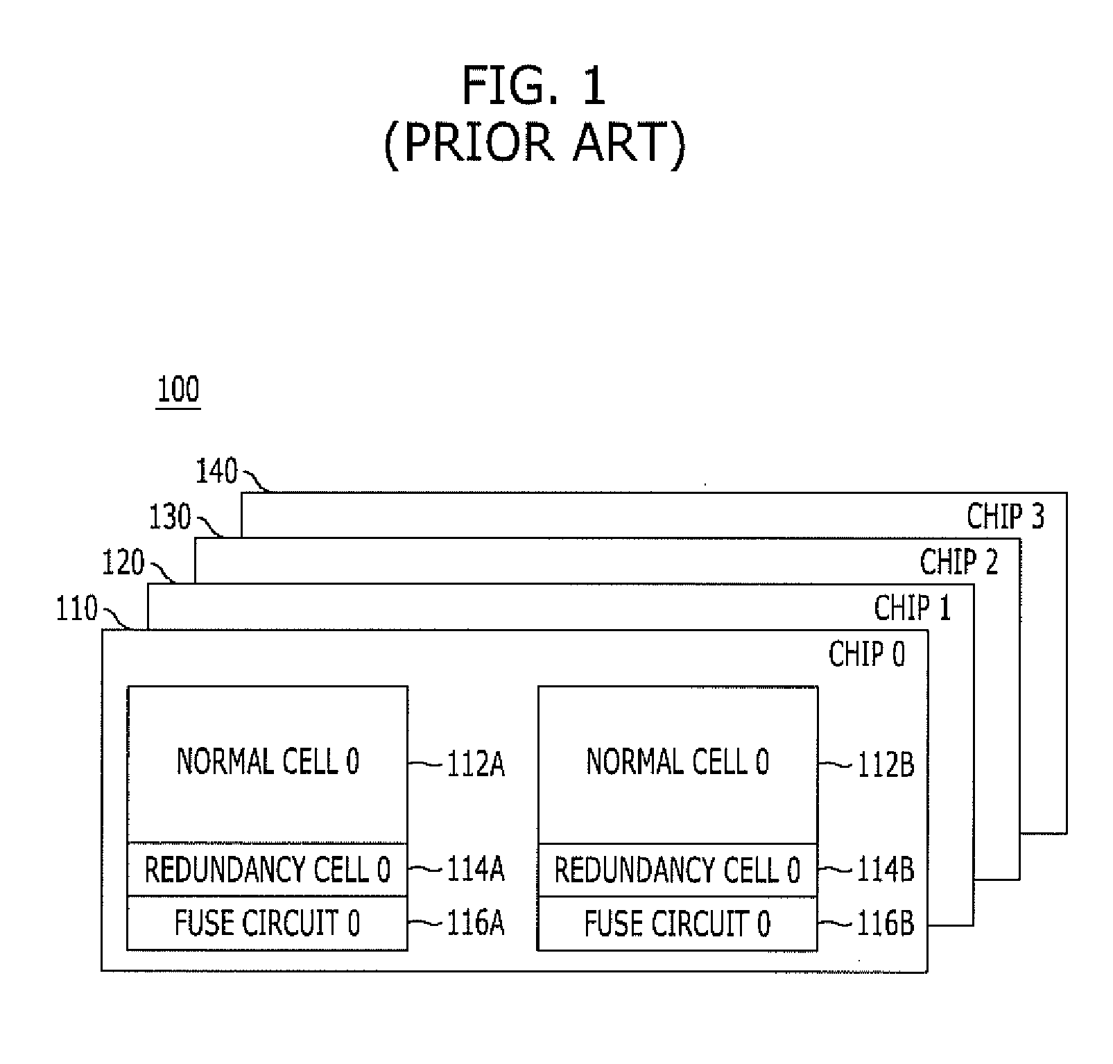
[0032]Hereinafter, a semiconductor chip including memory cells may be referred to as a memory chip and a semiconductor chip including a fuse circuit may be referred to as a repair chip.
[0033]FIG. 3 is a block...
PUM
 Abstract
Description
Claims
Application Information