Non-volatile memory unit cell with improved sensing margin and reliability

a non-volatile memory unit, sensing margin technology, applied in semiconductor devices, digital storage, instruments, etc., can solve problems such as misjudgment of data stored in non-volatile memory units, and achieve the effect of widening the memory window and improving the sensing margin

Active Publication Date: 2012-11-01
EMEMORY TECH INC
View PDF2 Cites 6 Cited by
  • Summary
  • Abstract
  • Description
  • Claims
  • Application Information

AI Technical Summary

Benefits of technology

[0010]Accordingly, the present invention is directed to non-volatile memory cells which each non-volatile memory unit cell comprises two identical memory elements with pre-determined connections and arrangements to serve as a purpose to improve sensing margin. In such way, these three type memory transistors can effectively widen the memory window or compensate for the un-expected electric leakage during data storage period.
[0012]In summary, the present invention provides an only-one-polysilicon layer non-volatile memory unit cell in which injection or removal of electrons or holes can be achieved to write or delete data in the manner of F-N tunneling, band-to-band tunneling hot electron (BBHE), band-to-band tunneling hot hole (BBHH), substrate hole, or channel hot electron (CHE). The non-volatile memory unit cell of the present invention comprises two identical memory elements with pre-determined connections and arrangements to serve as a purpose to improve sensing margin. In such way, the non-volatile memory unit cell can effectively widen the memory window or compensate for the un-expected electric leakage during data storage.

Problems solved by technology

Accordingly, the sensing result of the current sensor 220 may be incorrect which would result in misjudgement of the data stored in the non-volatile memory unit cell 210.

Method used


Image

  • Non-volatile memory unit cell with improved sensing margin and reliability
  • Non-volatile memory unit cell with improved sensing margin and reliability
  • Non-volatile memory unit cell with improved sensing margin and reliability

Examples


Embodiment Construction

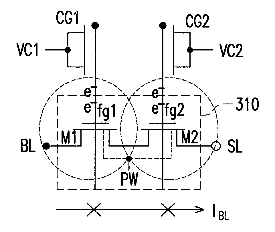
[0027]FIG. 3A illustrates an only-one-polysilicon layer non-volatile memory unit cell 300 according to one embodiment of the present invention. In some non-volatile memory technologies, two or more polysilicon layers are processed and stacked to achieve non-volatility purpose. In this embodiment, an only one polysilicon layer is discussed and addressed for a more cost-effective non-volatile memory solution and more suitable for embedded memory applications. Referring to FIG. 3A, the non-volatile memory unit cell 300 includes a transistor pair 310 and control gates CG1 and CG2. The transistor pair 310 includes a transistor M1 and a transistor M2 connected in series. The transistor M1 and the transistor M2 have a floating polysilicon gate fg1 and a floating polysilicon gate fg2, respectively, and the floating polysilicon gate fg1 and the floating polysilicon gate fg2 are electrically or physically isolated. The control gate CG1 is coupled to the floating polysilicon gates fg1 through ...


PUM


Abstract

An only-one-polysilicon layer non-volatile memory unit cell includes a first P-type transistor, a second P-type transistor, a N-type transistor pair, a first and second coupling capacitors is provided. The N-type transistor pair has a third transistor and a fourth transistor that are connected. The third transistor and the fourth transistor have a first floating polysilicon gate and a second floating polysilicon gate to serve as charge storage mediums, respectively. One end of the second coupling capacitor is connected to the gate of the second transistor and is coupled to the second floating polysilicon gate, the other end of the second coupling capacitor receives a second control voltage. One end of the second coupling capacitor is connected to the gate of the second transistor and is coupled to the second floating polysilicon gate, the other end of the second coupling capacitor receives a second control voltage.

Description

CROSS-REFERENCE TO RELATED APPLICATION[0001]This application is a divisional application of U.S. application Ser. No. 12 / 750,650, filed on Mar. 30, 2010, now pending. The entirety of the above-mentioned patent application is hereby incorporated by reference herein and made a part of this specification.BACKGROUND OF THE INVENTION[0002]1. Field of the Invention[0003]The present invention relates to an only-one-polysilicon layer non-volatile memory cell, especially for the methods to improve sensing margin and reliability.[0004]2. Description of Related Art[0005]A non-volatile memory is a memory capable of holding stored data when the memory is not supplied with power. There are currently two types of non-volatile memories, i.e. read only memory (ROM) and flash memory.[0006]FIG. 1 illustrates a conventional stacked polysilicon layers non-volatile memory unit cell and sensing of data thereof which was disclosed in U.S. Pat. No. 5,973,957. Referring to FIG. 1, floating polysilicon gates ...

Claims


Application Information

Patent Timeline
Patent Type & Authority Applications(United States)
IPC IPC(8): H01L27/06
CPCG11C16/0458H01L27/088G11C16/3418G11C16/28
Inventor CHEN, HSIN-MINGWANG, SHIH-CHENCHING, WEN-HAOLAI, YEN-HSINLU, HAU-YANYANG, CHING-SUNG
Owner EMEMORY TECH INC
Why Eureka
Try Eureka