SRAM read buffer with reduced sensing delay and improved sensing margin

a read buffer and sensing margin technology, applied in the field of memory devices, can solve the problems of reducing supply voltage, consuming low power, and sram cells may exhibit reduced performance, and achieve the effects of increasing ioff, increasing similarity, and increasing sensing delay

Active Publication Date: 2015-02-05
QUALCOMM INC +1
View PDF18 Cites 7 Cited by
  • Summary
  • Abstract
  • Description
  • Claims
  • Application Information

AI Technical Summary

Benefits of technology

[0004]Certain SRAM configurations with a reduced supply voltage utilize a read buffer. The read buffer may be coupled between an SRAM cell and a bit line. The read buffer may “buffer” the SRAM cell during read operations, such as by providing isolation between the bit line and a storage node of the SRAM cell holding the data value to be read. However, the read buffer may degrade a sensing margin associated with reading a logical high voltage (e.g., a “one” bit value), may increase a sensing delay associated with reading a logical low voltage (e.g., a “zero” bit value), or a combination thereof. For example, the read buffer may be associated with a large leakage current that reduces an on-current-to-off-current ratio Ion / Ioff associated with the SRAM cell (e.g., by increasing Ioff), degrading the sensing margin associated with sensing the logical high voltage due to increased similarity between on and off states. Some SRAM configurations attempt to improve the sensing margin by using particular configurations (e.g., a “buffer foot”) in connection with the read buffer. However, these configurations may increase a delay associated with sensing the logical low voltage, such as by increasing a capacitance between the SRAM cell and the bit line.

Problems solved by technology

Increasingly, users expect mobile devices to include high (e.g., “fast”) performance while also consuming low power (e.g., having long battery life).
As supply voltages decrease, SRAM cells may exhibit reduced performance.
For example, reduced supply voltages may be associated with decreased read stability of SRAM cells (e.g., where a value stored by an SRAM cell is more susceptible to being corrupted by noise).
That is, a data value stored at the SRAM cell may be more susceptible to noise during a read operation than while holding the data value during non-read operational states, thus potentially causing poor performance (e.g., data loss) of an electronic device that includes the SRAM cell.
However, the read buffer may degrade a sensing margin associated with reading a logical high voltage (e.g., a “one” bit value), may increase a sensing delay associated with reading a logical low voltage (e.g., a “zero” bit value), or a combination thereof.
However, these configurations may increase a delay associated with sensing the logical low voltage, such as by increasing a capacitance between the SRAM cell and the bit line.

Method used


Image

  • SRAM read buffer with reduced sensing delay and improved sensing margin
  • SRAM read buffer with reduced sensing delay and improved sensing margin
  • SRAM read buffer with reduced sensing delay and improved sensing margin

Examples


Embodiment Construction

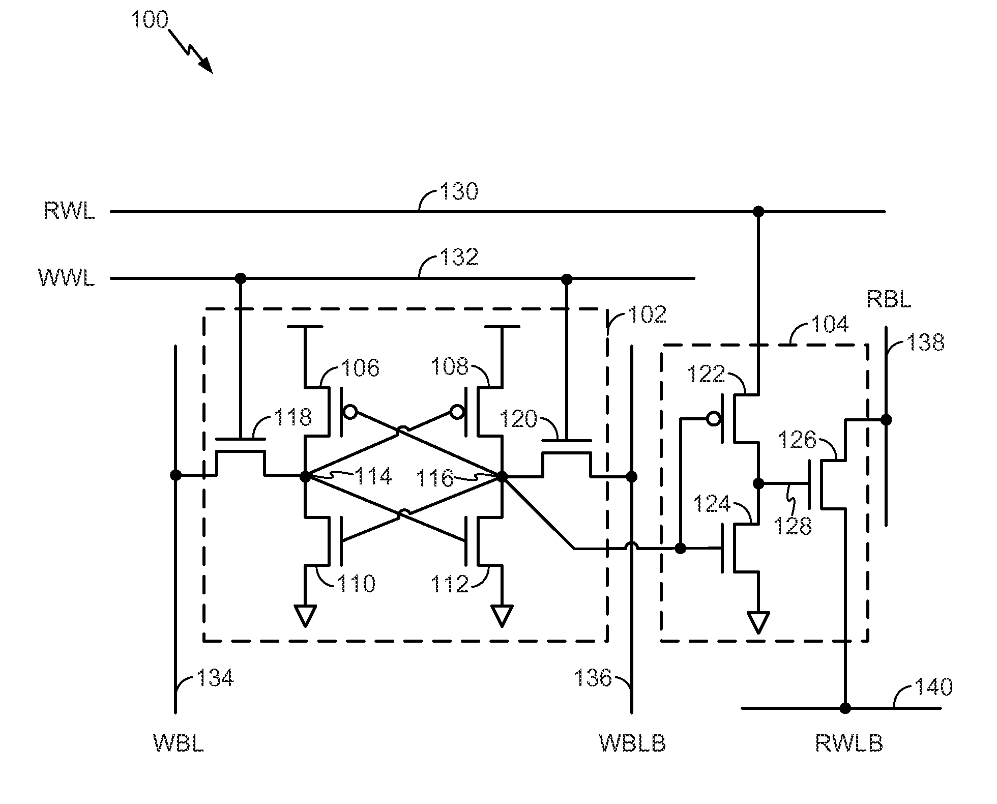
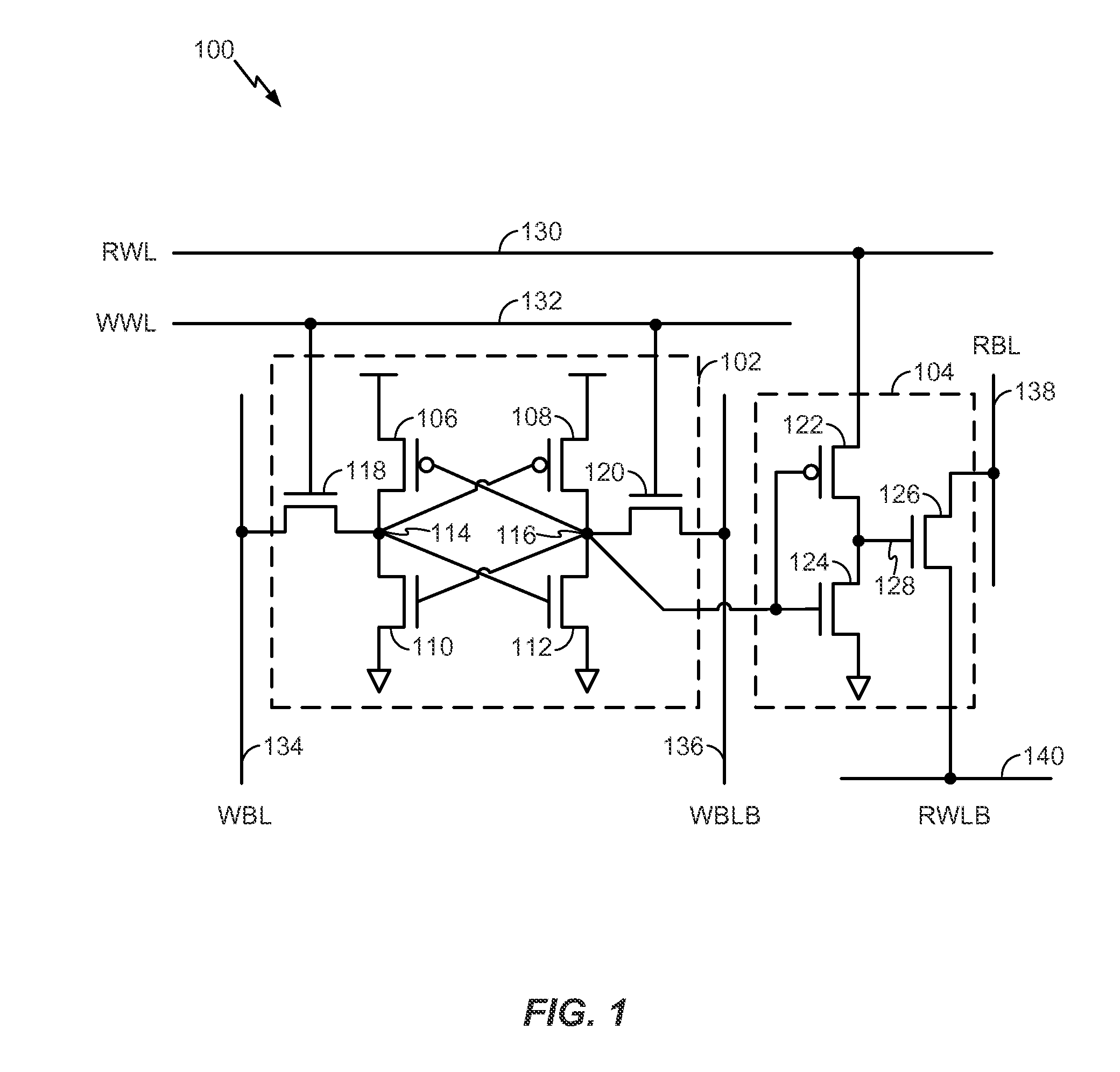
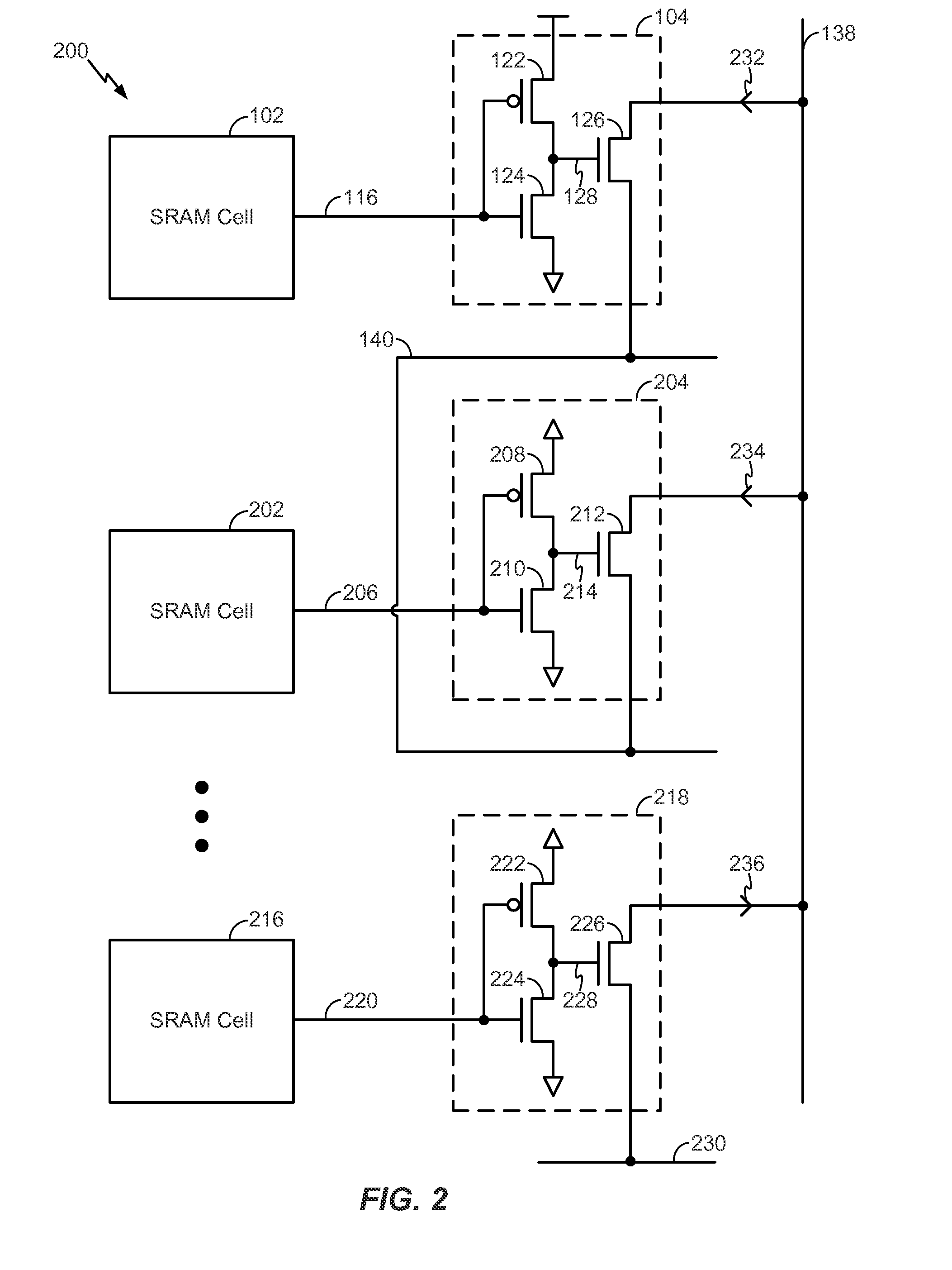
[0019]Referring to FIG. 1, a particular illustrative embodiment of a device is depicted and generally designated 100. The device 100 includes a static random access memory (SRAM) cell 102. The device 100 further includes a read buffer 104 coupled to the SRAM cell 102.

[0020]The SRAM cell 102 may include a pair of cross-coupled inverters. For example, in FIG. 1, the SRAM cell 102 includes a first inverter formed by a p-type metal-oxide-semiconductor field-effect transistor (pMOSFET) 106 coupled to an n-type metal-oxide-semiconductor field-effect transistor (nMOSFET) 110. The first inverter is cross-coupled with a second inverter formed by a pMOSFET 108 coupled to an nMOSFET 112. The pMOSFET 106 is coupled to the nMOSFET 110 via a node 114. The pMOSFET 108 is coupled to the nMOSFET 112 via a node 116.

[0021]The SRAM cell 102 may further include multiple access transistors. For example, the SRAM cell 102 includes an access transistor 118 and an access transistor 120. The access transisto...


PUM


Abstract

A device includes a static random access memory (SRAM) cell and a read buffer coupled to an output of the SRAM cell. The read buffer includes an inverter and a switch. An input of the inverter is responsive to the output of the SRAM cell. A control terminal of the switch is responsive to an output of the inverter.

Description

I. FIELD[0001]The present disclosure is generally related to memory devices and more particularly to read buffers for memory devices.II. DESCRIPTION OF RELATED ART[0002]Advances in technology have resulted in smaller and more powerful electronic devices. For example, there currently exist a variety of mobile devices, such as wireless telephones, personal digital assistants (PDAs), and paging devices. The mobile devices may be small, lightweight, and easily carried by users. Wireless telephones, such as cellular telephones and Internet Protocol (IP) telephones, can communicate voice and data packets over wireless networks. Further, many wireless telephones include other types of devices that are incorporated therein. For example, a wireless telephone can also include a digital still camera, a digital video camera, a digital recorder, and an audio file player. Also, wireless telephones can process executable instructions, including software applications, such as a web browser applicat...

Claims


Application Information

Patent Timeline
Patent Type & Authority Applications(United States)
IPC IPC(8): G11C11/419G06F17/50
CPCG06F17/5072G11C11/419G11C8/16G11C11/412G06F30/392
Inventor JUNG, SEONG-OOKYANG, YOUNGHWISONG, STANLEY SEUNGCHULWANG, ZHONGZEYEAP, CHOH FEI
Owner QUALCOMM INC
Why Eureka
Try Eureka