Method for making light emitting diode

a technology of light-emitting diodes and methods, which is applied in the direction of semiconductor devices, electrical equipment, nanotechnology, etc., can solve the problems of reduced light-emitting from the active layer, low extraction efficiency of leds, and reduced light-emitting efficiency

Active Publication Date: 2012-11-01
TSINGHUA UNIV +1
View PDF1 Cites 17 Cited by
  • Summary
  • Abstract
  • Description
  • Claims
  • Application Information

AI Technical Summary

Problems solved by technology

However, extraction efficiency of LEDs is low for the following reasons: first, the typical semiconductor materials have a higher refraction index than that of air, therefore, large-angle lights emitted from the active layer may be internally reflected in LEDs, so that a large portion of the lights emitted from the active layer will remain in the LEDs; second, the cur

Method used


Image

  • Method for making light emitting diode
  • Method for making light emitting diode
  • Method for making light emitting diode

Examples


Embodiment Construction

[0023]The disclosure is illustrated by way of example and not by way of limitation in the figures of the accompanying drawings in which like references indicate similar elements. It should be noted that references to “an” or “one” embodiment in this disclosure are not necessarily to the same embodiment, and such references mean at least one.

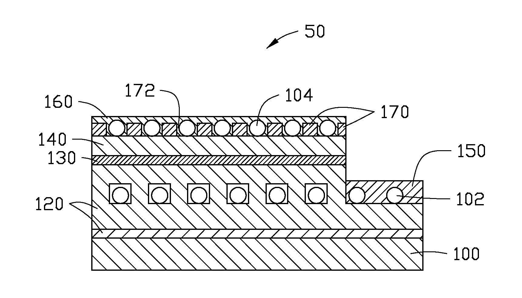
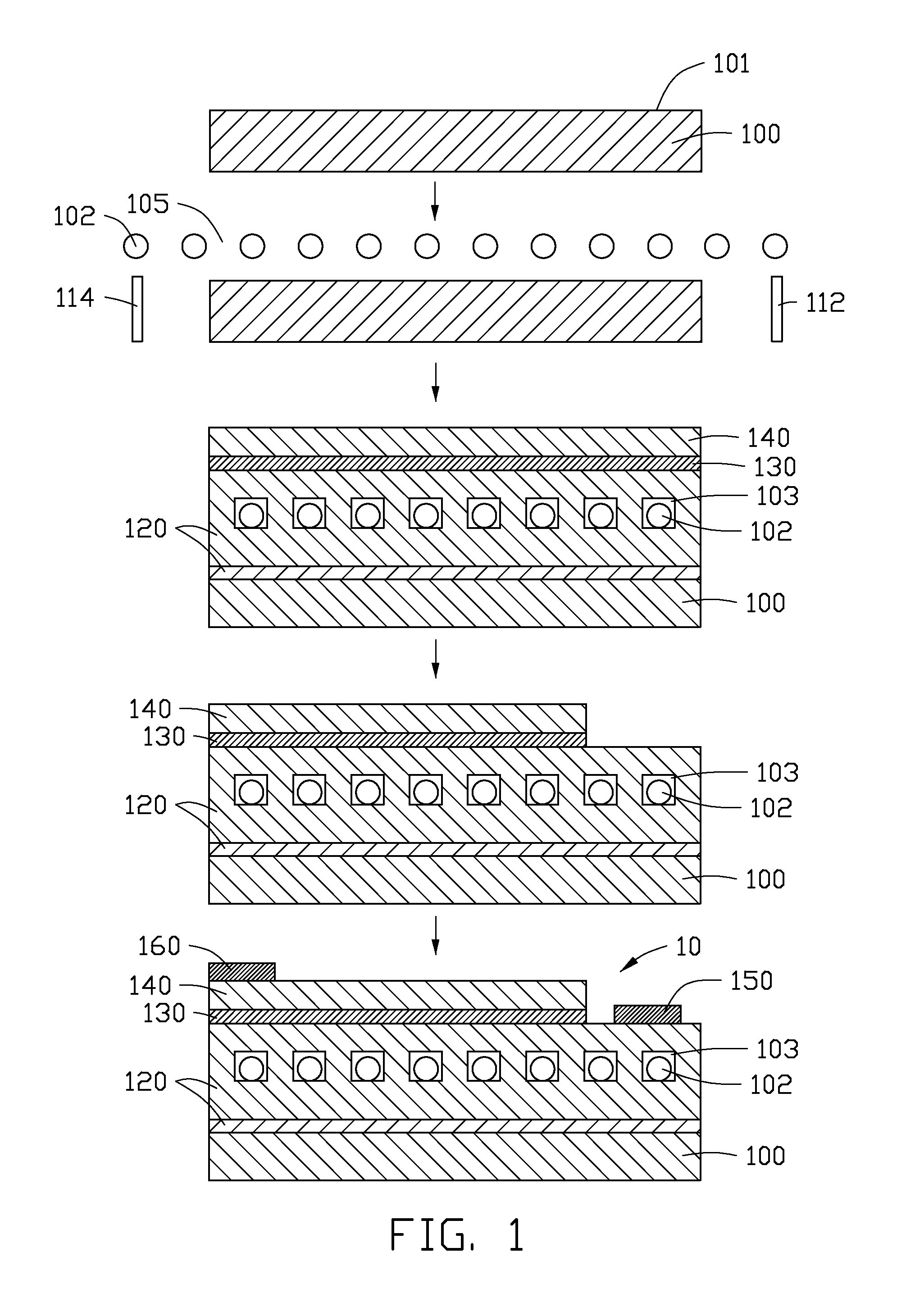
[0024]Referring to FIG. 1, a method for making an LED of one embodiment includes the following steps:

[0025]S11, providing a substrate 100 having an epitaxial growth surface 101;

[0026]S12, suspending a carbon nanotube layer 102 above the epitaxial growth surface 101; and

[0027]S13, growing a first semiconductor layer 120, an active layer 130, and a second semiconductor layer 140 on the epitaxial growth surface 101 in that order, in which the carbon nanotube layer 102 is enclosed in the first semiconductor layer 120;

[0028]S14, etching a portion of the second semiconductor layer 140 and the active layer 130 to expose a portion of the first semiconduc...


PUM


Abstract

A method for making light emitting diode, the method includes the following steps. First, a substrate having an epitaxial growth surface is provided. Second, a carbon nanotube layer is suspended above the epitaxial growth surface. Third, a first semiconductor layer, an active layer and a second semiconductor layer are grown on the epitaxial growth surface in that order. Fourth, a portion of the second semiconductor layer and the active layer is etched to expose a portion of the first semiconductor layer. Fifth, a first electrode is prepared on the first semiconductor layer and a second electrode is prepared on the second semiconductor layer.

Description

CROSS-REFERENCE TO RELATED APPLICATIONS[0001]This application claims all benefits accruing under 35 U.S.C. §119 from China Patent Application No. 201110110728.6, filed on Apr. 29, 2011, in the China Intellectual Property Office, the contents of which are hereby incorporated by reference. This application is related to commonly-assigned applications entitled “METHOD FOR MAKING LIGHT EMITTING DIODE”, filed ______ (Atty. Docket No. US39404); “LIGHT EMITTING DIODE”, filed ______ (Atty. Docket No. US39405); “METHOD FOR MAKING LIGHT EMITTING DIODE”, filed ______ (Atty. Docket No. US39406); “LIGHT EMITTING DIODE”, filed ______ (Atty. Docket No. US39408); “METHOD FOR MAKING LIGHT EMITTING DIODE”, filed ______ (Atty. Docket No. US39409); “LIGHT EMITTING DIODE”, filed ______ (Atty. Docket No. US39410); “LIGHT EMITTING DIODE”, filed ______ (Atty. Docket No. US39411); “LIGHT EMITTING DIODE”, filed ______ (Atty. Docket No. US39413); “METHOD FOR MAKING LIGHT EMITTING DIODE”, filed ______ (Atty. D...

Claims


Application Information

Patent Timeline
IPC IPC(8): H01L33/62B82Y40/00
CPCH01L21/02521H01L33/0062H01L21/02546H01L21/02579H01L21/0262H01L21/02642H01L21/02647H01L33/007H01L33/641H01L21/0237H01L21/0242H01L21/02458H01L51/0048B82Y40/00H01L33/36H01L33/64Y10S977/742H01L33/20H01L2924/0002H01L21/0254B82Y10/00H01L2924/00H10K85/221
Inventor WEI, YANGFAN, SHOU-SHAN
Owner TSINGHUA UNIV
Why Eureka
Try Eureka