Bus line designs for large-area OLED lighting

a technology of oled lighting and bus line, which is applied in the direction of organic semiconductor devices, basic electric elements, nanotechnology, etc., can solve the problems of difficult to dispose uniform thin films over the bus line, reduce device efficacy, and non-uniformity of illumination, so as to minimize pl, maximize ff, and maximize u

Active Publication Date: 2012-11-15
UNIVERSAL DISPLAY
View PDF8 Cites 33 Cited by
  • Summary
  • Abstract
  • Description
  • Claims
  • Application Information

AI Technical Summary

Benefits of technology

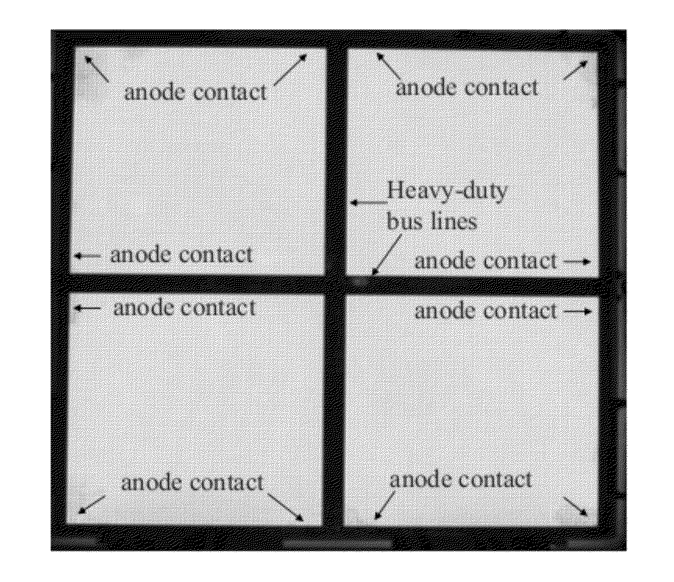
[0020]In view of the foregoing, it has been recognized that it is important not to pattern bus lines with an excessively large area. According to aspects of the invention, systems, and methods for the design and fabrication of OLEDs, including large-area OLEDs with metal bus lines, are provided. In embodiments various bus line design rules for large area OLED light panels may include mathematical models developed to optimize bus line design and/or layout on large area OLED light panels. In embodiments, for a given panel area dimension, target luminous emittance, OLED device structure and efficiency (as given by the JVL characteristics of an equivalent small area pixel), and electrical resistivity and ...

Problems solved by technology

In large area OLED light panels, potential drops due to significant electrode resistances can cause luminance non-uniformity and reduce device efficacy.
However, in practice, there is a finite height at which it is practical to deposit ...

Method used


Image

  • Bus line designs for large-area OLED lighting
  • Bus line designs for large-area OLED lighting
  • Bus line designs for large-area OLED lighting

Examples


Embodiment Construction

[0084]It is understood that the invention is not limited to the particular methodology, protocols, and reagents, etc., described herein, as these may vary as the skilled artisan will recognize. It is also to be understood that the terminology used herein is used for the purpose of describing particular embodiments only, and is not intended to limit the scope of the invention. It also is be noted that as used herein and in the appended claims, the singular forms “a,”“an,” and “the” include the plural reference unless the context clearly dictates otherwise. Thus, for example, a reference to “a bus line” is a reference to one or more bus lines and equivalents thereof known to those skilled in the art.

[0085]Unless defined otherwise, all technical and scientific terms used herein have the same meanings as commonly understood by one of ordinary skill in the art to which the invention pertains. The embodiments of the invention and the various features and advantageous details thereof are e...


PUM


Abstract

Systems, and methods for the design and fabrication of OLEDs, including large-area OLEDs with metal bus lines, are provided. Various bus line design rules for large area OLED light panels may include mathematical models developed to optimize bus line design and/or layout on large area OLED light panels. For a given panel area dimension, target luminous emittance, OLED device structure and efficiency (as given by the JVL characteristics of an equivalent small area pixel), and electrical resistivity and thickness of the bus line material and electrode onto which the bus lines are disposed, a bus line pattern may be designed such that Fill Factor (FF), Luminance Uniformity (U) and Power Loss (PL) may be optimized. One general design objective may be to maximize FF, maximize U and minimize PL. Another approach may be, for example, to define minimum criteria for U and a maximum criteria for PL, and then to optimize the bus line layout to maximize FF. OLED panels including bus lines with different resistances (R1) along a length of the bus line are also described.

Description

FIELD OF THE INVENTION[0001]The present invention relates to systems, and processes for fabricating OLED lighting panels, and particularly for designing and forming metal bus lines as may be used in large-area OLED lighting panels.BACKGROUND[0002]Opto-electronic devices that make use of organic materials are becoming increasingly desirable for a number of reasons. Many of the materials used to make such devices are relatively inexpensive, so organic opto-electronic devices have the potential for cost advantages over inorganic devices. In addition, the inherent properties of organic materials, such as their flexibility, may make them well suited for particular applications such as fabrication on a flexible substrate. Examples of organic opto-electronic devices include organic light emitting devices (OLEDs), organic phototransistors, organic photovoltaic cells, and organic photodetectors. For OLEDs, the organic materials may have performance advantages over conventional materials. For...

Claims


Application Information

Patent Timeline
IPC IPC(8): H01L33/08H01L33/62
CPCH01L51/0092H01L51/0072H01L51/0058H01L51/0046H01L2251/5361B82Y10/00H01L2051/0063H01L51/5228H01L51/0068H01L51/008H01L51/0067H01L51/5212H01L51/5203H01L2924/0002H10K85/211H10K85/655H10K85/6565H10K85/626H10K85/322H10K85/654H10K85/381H10K85/6572H10K50/805H10K50/814H10K50/824H01L2924/00H10K59/84H10K50/11H10K50/81H10K50/82H10K59/86H01L23/5256H01L23/528
Inventor PANG, HUIQINGLEVERMORE, PETERKRALL, EMORYRAJAN, KAMALABURROWS, PAUL E.
Owner UNIVERSAL DISPLAY
Why Eureka
Try Eureka