

Semiconductor device and method of manufacturing the same
- Summary
- Abstract
- Description
- Claims
- Application Information
AI Technical Summary
Benefits of technology
Problems solved by technology
Method used
Image

Examples
Embodiment Construction
.”
BRIEF DESCRIPTION OF THE DRAWINGS
[0023]The above and other aspects, features, and other advantages of the subject matter of the present disclosure will be more clearly understood from the following detailed description taken in conjunction with the accompanying drawings, in which:
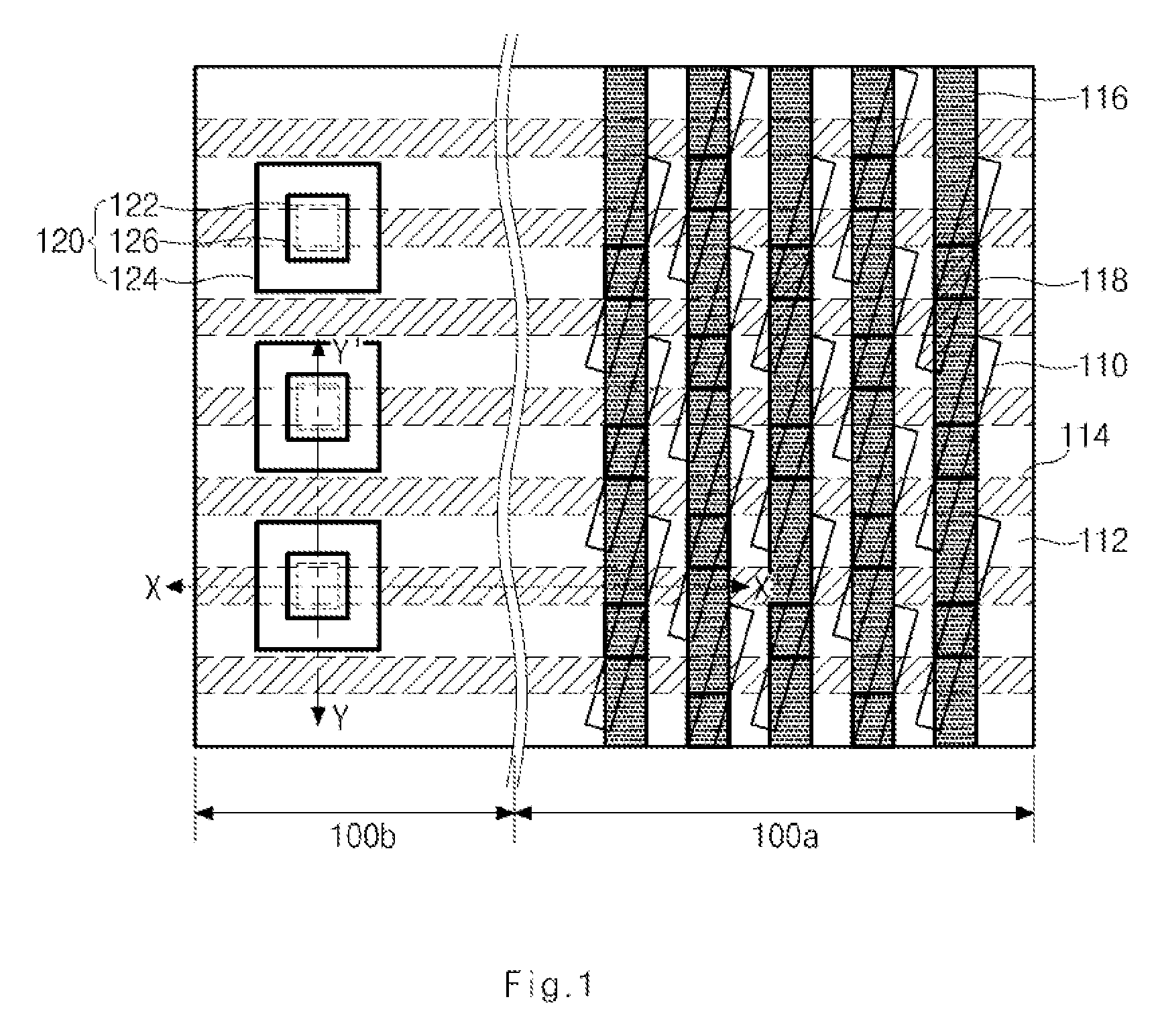
[0024]FIG. 1 is a plan view illustrating a structure of a semiconductor device according to an exemplary embodiment of the present invention;
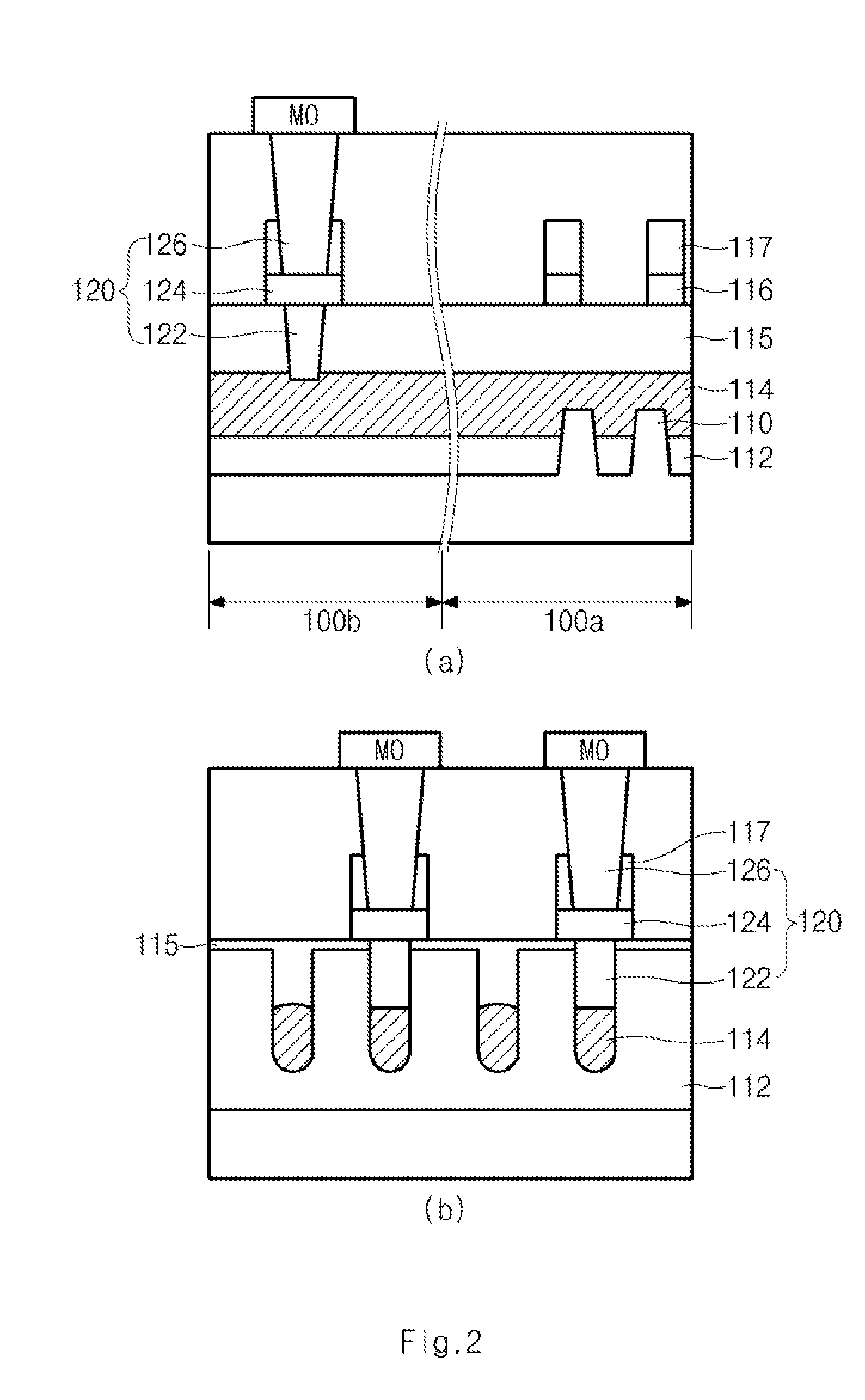
[0025]FIG. 2 is a cross-section view of the semiconductor device of FIG. 1, wherein (a) is a cross-sectional view taken along the line X-X′ of FIG. 1 and (b) is a cross-sectional view taken along the line Y-Y′ of FIG. 1; and
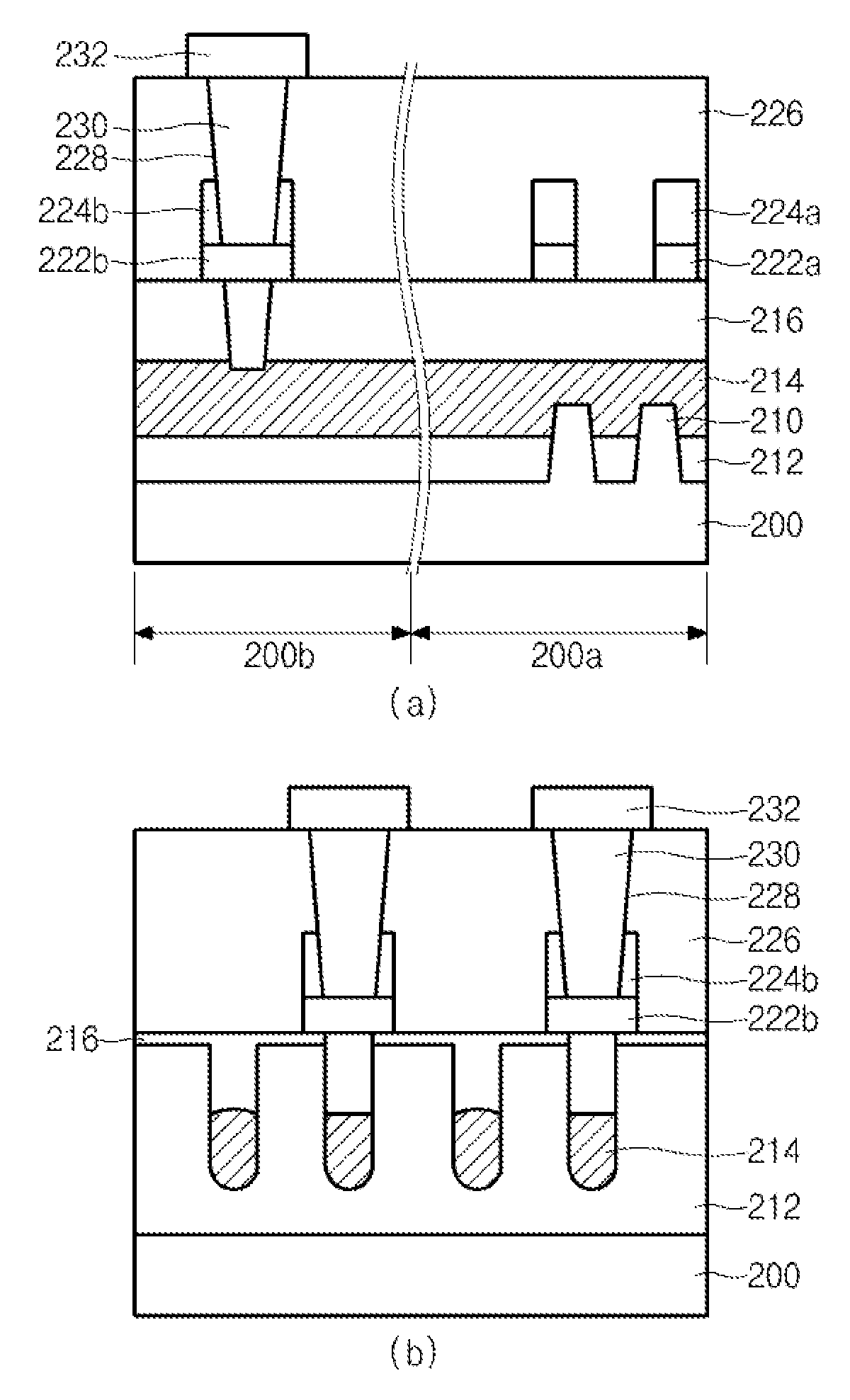
[0026]FIGS. 3 to 7 are cross-sectional views illustrating a process of manufacturing the semiconductor device of FIG. 2 according to an exemplary embodiment of the present invention, wherein, respectively, (a) is a cross-sectional view taken along the line X-X′ of FIG. 1, and respectively, (b) is a cross-sectional view taken along the line Y-Y′ of...
PUM
 Abstract
Description
Claims
Application Information