Electronic device including a patch antenna and photovoltaic layer and related methods
- Summary
- Abstract
- Description
- Claims
- Application Information
AI Technical Summary
Problems solved by technology
Method used
Image
Examples
Embodiment Construction
[0028]The present invention will now be described more fully hereinafter with reference to the accompanying drawings, in which preferred embodiments of the invention are shown. This invention may, however, be embodied in many different forms and should not be construed as limited to the embodiments set forth herein. Rather, these embodiments are provided so that this disclosure will be thorough and complete, and will fully convey the scope of the invention to those skilled in the art. Like numbers refer to like elements throughout, and prime and multiple notation is used to indicate similar elements in alternative embodiments.
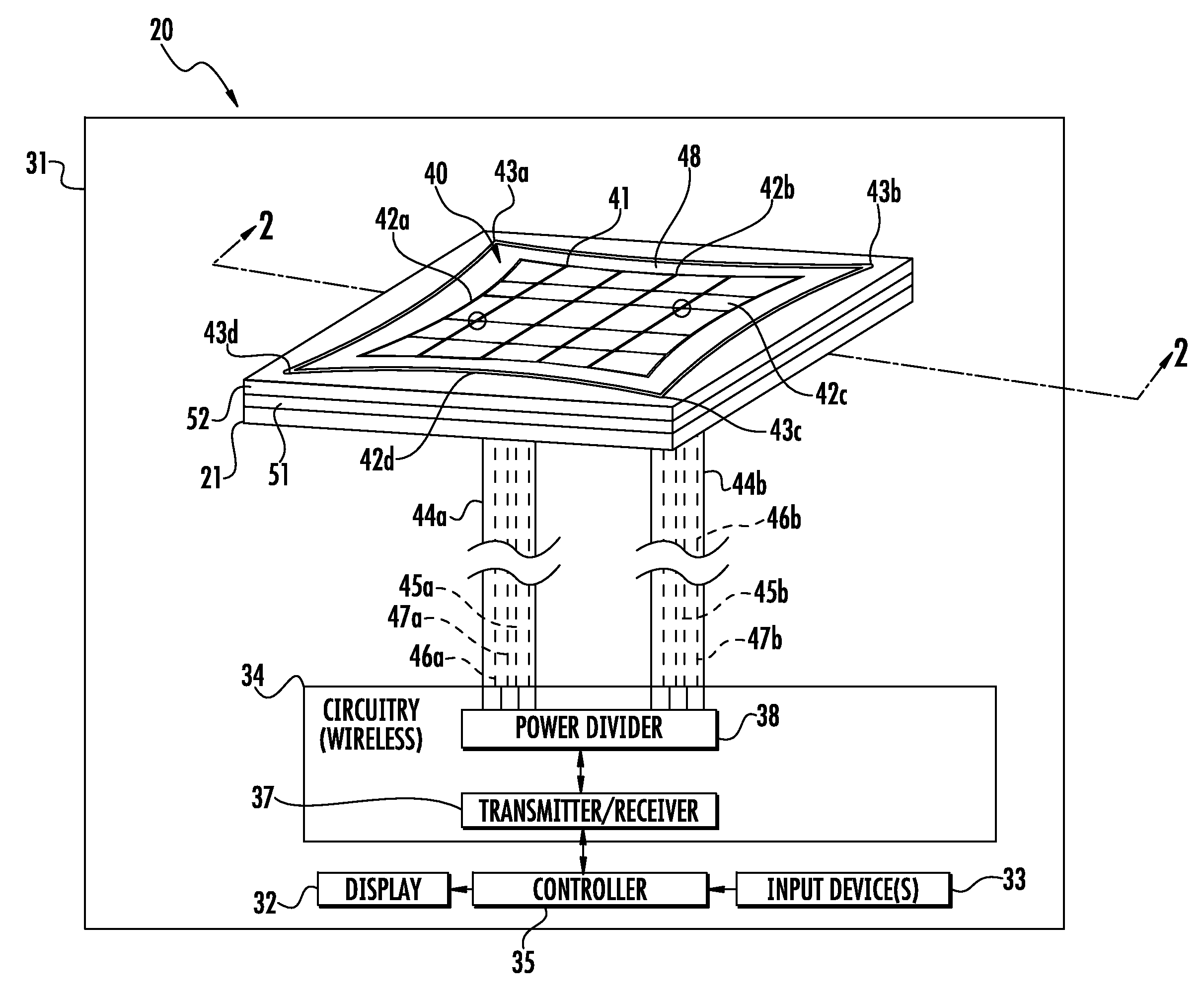
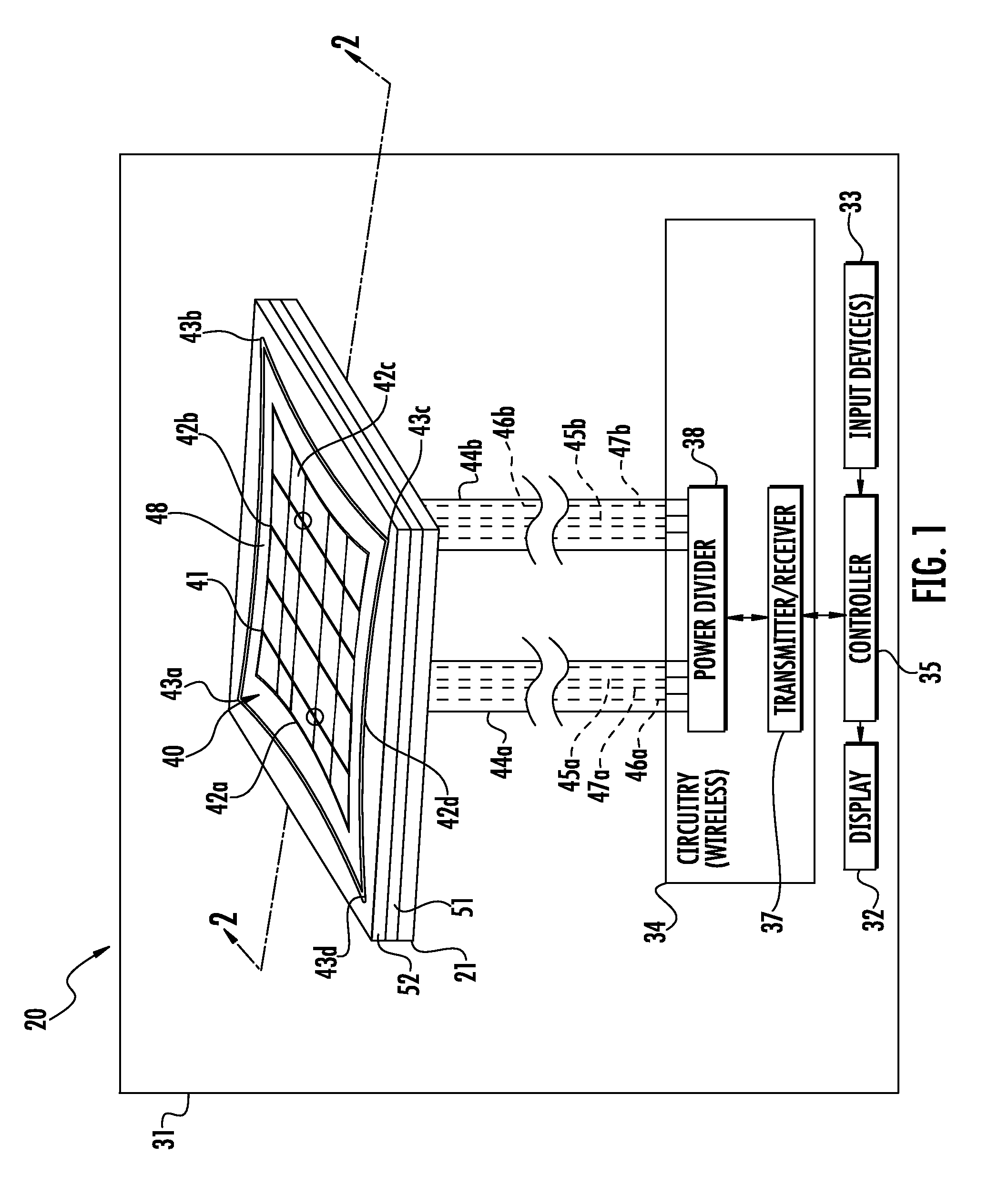
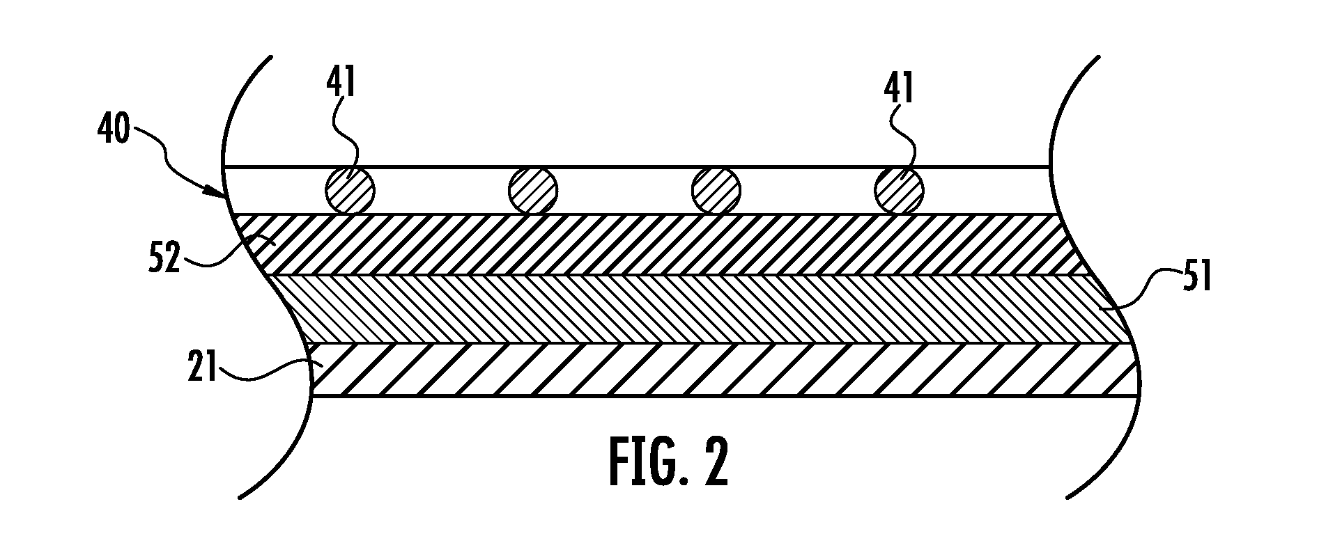
[0029]Referring initially to FIGS. 1-3, an electronic device 20 illustratively includes a housing 31. The electronic device also includes circuitry 34 carried by the housing 31. The electronic device 20 also includes input devices 33 and a display 32 carried by the housing 31. The circuitry 34 also includes a power divider 38 a receiver and / or transmitter 37 co...
PUM
| Property | Measurement | Unit |
|---|---|---|
| Mass | aaaaa | aaaaa |
| Fraction | aaaaa | aaaaa |
| Fraction | aaaaa | aaaaa |
Abstract
Description
Claims
Application Information


