Storage control apparatus for controlling data writing and deletion to and from semiconductor storage device, and control method and storage medium therefor

Inactive Publication Date: 2012-11-15
CANON KK
View PDF18 Cites 9 Cited by
  • Summary
  • Abstract
  • Description
  • Claims
  • Application Information

AI Technical Summary

Benefits of technology

[0012]With this invention, it is possible to properly delete data dispersedly stored in the semiconductor storage device with wear leveling.

Problems solved by technology

Accordingly, when a delete instruction is given to the LBA from the host, data written in the PBA that is indicated by the latest connection information can be deleted, however, one or more pieces of data previously written in one or more PBAs that are unknown from the latest connection information cannot be deleted and are left remaining on the flash memory, which poses a problem.

Method used


Image

  • Storage control apparatus for controlling data writing and deletion to and from semiconductor storage device, and control method and storage medium therefor
  • Storage control apparatus for controlling data writing and deletion to and from semiconductor storage device, and control method and storage medium therefor
  • Storage control apparatus for controlling data writing and deletion to and from semiconductor storage device, and control method and storage medium therefor

Examples


first embodiment

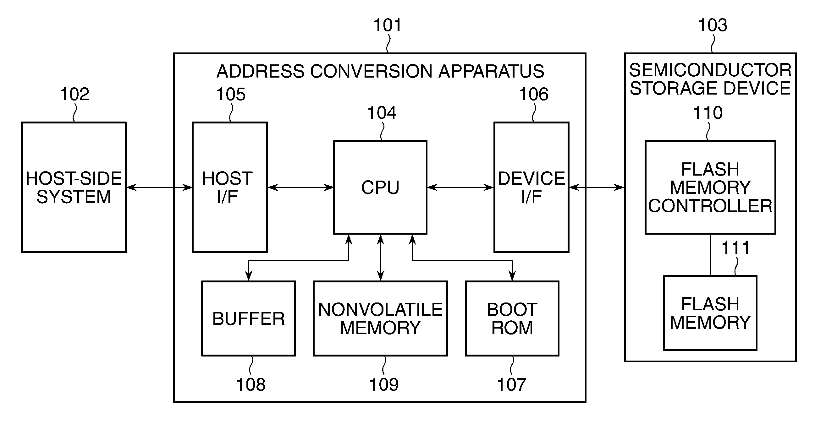
[0027]FIG. 1 schematically shows, in block diagram, the construction of an address conversion apparatus serving as a storage control apparatus according to a first embodiment of this invention.

[0028]In FIG. 1, reference numeral 101 denotes the address conversion apparatus interposed between a host-side system 102 and a semiconductor storage device 103. The address conversion apparatus 101 includes a CPU 104, boot ROM 107, buffer 108, nonvolatile memory 109, host I / F 105 connected to the host-side system 102, and device I / F 106 connected to the semiconductor storage device 103.

[0029]The CPU 104 is connected via the host I / F 105 to the host-side system 102 and connected via the device I / F 106 to the semiconductor storage device 103, and performs a bridge process between the host-side system 102 and the semiconductor storage device 103.

[0030]The CPU 104 is also connected with the boot ROM 107, buffer 108, and nonvolatile memory 109. The boot ROM 107 stores a firmware for activating the...

second embodiment

[0075]In a second embodiment of this invention, the flash memory controller is configured to have a construction similar to that of the address conversion apparatus and achieve the address conversion function, unlike the first embodiment where the address conversion apparatus 101 having the address conversion function is provided independently of the semiconductor storage device 103 and the host-side system 102. In the following, a description of points common to the first and second embodiments will be omitted.

[0076]FIG. 6 schematically shows a storage control apparatus according to the second embodiment.

[0077]In FIG. 6, reference numeral 606 denotes an assembly of a flash memory controller 610 as a storage control apparatus and a flash memory 611 as a semiconductor storage device. The flash memory controller 610 includes a CPU 601 and includes a buffer 602, nonvolatile memory 603, boot ROM 604, and host I / F 605, which are connected to the CPU 601. The host-side system. 102 is conn...

third embodiment

[0093]In a third embodiment of this invention, unlike the first embodiment where the address conversion apparatus is provided independently of the semiconductor storage device and the host-side system, the CPU and memory of the host-side system are used instead of using the CPU and buffer of the address conversion apparatus, and the address conversion function is achieved by software running on the host-side system.

[0094]FIG. 10 schematically shows the construction of a storage control apparatus according to this embodiment.

[0095]In FIG. 10, reference numeral 810 denotes the host-side system as the storage control apparatus. The host-side system 810 includes a CPU 801 and includes a buffer 802, nonvolatile memory 803, boot ROM 804, and device I / F 805, which are connected to the CPU 801. A flash memory controller of a semiconductor storage device 811 is connected to the device I / F 805. The flash memory controller has a map for wear leveling and is connected to a flash memory. It shou...


PUM


Abstract

A storage control apparatus capable of properly deleting data dispersedly stored in a semiconductor storage device with wear leveling. The storage control apparatus converts an address given with a write instruction, among addresses of the semiconductor storage device, into another address, holds address conversion information that associates the before- and after-conversion addresses with each other, and controls the semiconductor storage device to write data into the after-conversion address. When a delete instruction is given, the storage control apparatus controls the semiconductor storage device in accordance with the address conversion information to delete data stored in an after-conversion address associated with an address given with the delete instruction.

Description

BACKGROUND OF THE INVENTION[0001]1. Field of the Invention[0002]The present invention relates to a storage control apparatus for controlling data writing and deletion to and from a semiconductor storage device such as a flash memory, and relates to a control method for the storage control apparatus and a storage medium storing a program for causing a computer to execute the control method.[0003]2. Description of the Related Art[0004]Recently, there has been used a semiconductor storage device that includes a flash memory and a flash memory controller for controlling the flash memory. Since the flash memory is limited in the number of writing times and in the number of deletion times due to its internal structure, load balancing (wear leveling) is performed to prevent concentrated writing to a particular portion of the flash memory.[0005]Among various wear leveling methods, there is often used a wear leveling method where an address is operated at the time of writing to the flash mem...

Claims


Application Information

Patent Timeline
Patent Type & Authority Applications(United States)
IPC IPC(8): G06F12/00
CPCG06F12/0246G06F2212/7211G06F2212/7201
Inventor ASANO, KOHEIINABA, KEISHISHIMIZU, KOJIUMIMURA, KIYOKAZUNAYA, YUJIKONOSU, YUICHI
Owner CANON KK
Why Eureka
Try Eureka